SERVICE MANUAL
CODE: OOZMZ 3500SM/E
PERSONAL COMPUTER
MODEL
CONTENTS
13.Circuit diagram & P.W.B Parts list & Guide
SHARP CORPORATION
SERVICE MANUAL
CODE: OOZMZ 3500SM/E
PERSONAL COMPUTER
MODEL
CONTENTS
13.Circuit diagram & P.W.B Parts list & Guide
SHARP CORPORATION

M 7 3500
1. SPECIFICATIONS
Light pen
Other I/F
Other functions
Software
Basic CP/M
CP/M Expanded CP/M
Intstruction Manual Accessories master floppy disk
power cord

MZ3500
MZ1K03: U.K. keyboard (ISO).
MZ1K05: French keyboard
80C49 or 8749
4049x2,4514
Mechanical contact key, with life of 10,000,000 operations.
61 Ten key 15 Function keys 6 Definable keys 10
1
Interfacing cables
Specification
Other
Cabinet
For data transfer with the CPU (serial) and power supply (transmission under 15,000 baud)
Use of coiled cable with
Automatic repeat occurs 0.64 seconds after
Repeat function. . . . . 2
Indicators (4 LED's) POWER, Alphanumeric keys
Keyboard layout
Refer to the page TIN "CIRCUIT DIAGRAM"
Expansion unit for the
The expansion box will accomodate up to four option boards.
Number of slots: 4 slots
Slot connector.
Specifications Area of the slot inserting option board: 140.5 x 140
Slot for option and slot number
MZ3500
Expansion unit
Screw (1)
Outline
Optional board used graphic display functions with the
The
GDC Graphic controller
MPD7220
LSI
vinrn HAM
Basic
Expansion (optional)
16KDRAM x 16 (32KB)
Specifications
Graphic functions (Color must be specified for each dot. when the color video unit is in use)
~~~~~
640 x 200 green monitor
640 x 200 color monitor
640 x 400 green monitor
640 x 400 color monitor
Software
MZ3500
Outline
Specifications
Optional board for memory expantion of the
This option plug into the expantion box in slot 1 or 3.
- 4 -

MZ3500
Outline
Specifications
High resolution MZ
Video tube
Display capacity
Display size
Input signals
Power supply
Cabinet
Adjusting knobs Accessories
CPU connection cable andpower cord and Tilt stand
12", 90" deflection
640 horizontal dots,
400 vertical lines
47 8 Hz
7.2kg
r
- 5-
MZ3500
Keyboard
Printer '
IO2824E I
I I
Option MFDI
I
I I
6

MZ3500
2. SOFTWARE (MEMORY) CONFIGURATION
Memory will be operated under four states of SDO ~ SD3, depending on the hardware and software configurations. In the paragraphs to follow, description will be made for those four states.
MAIN CPU
MAS 00 1
MA2 001
MAI 001
MAO 011
SDO can only exist immediately after power on, and the system executes IPL under this condition and that the system thus loaded will automatically assign memory area
for SD1, SD2. and SD3.
SUB CPU
MS1 = ?? (D
MSO = 0 (L)
FFFF
V FFFF T
? IRAM(COM^
RAMA RAMA
cooo
BFFF
*7

M 7. 3500
Operational description
(1)Upon reset after power on, the main CPU loads the contents of the initial program loader (IPL) into RAM starting at address 4000H, during which time reset is applied to the
TIMING OF RESET SIGNAL
Vtc-
S Y S K E S -
SKES-
(2)The main CPU then terminates resetting the sub CPU and starts the
(3)The main CPU then send the memory allocation (state) to SD1, and starts to load DOS from the system floppy disk.
Signal generated from the
CR network and power supply
Output signal from the main CPU port
MAIN CPU
START
Memory Map Data:
1.
2.The
3.
CPU.
a.Main CPU reset time
b.Main CPU IPL load time
4.Memories other than described above cannot be accessed under the SDOstate.
5.Bank select, MAO~MA3, is used within the address range

1.An 8KB ROM (2764 or mask ROM equivalent) is used for the
2.When the system reset signal turns from low to high state after power on, the main CPU starts to operate At this stage, the
3.The CPU starts from address OOOOIROM address 10000)
4.The main CPU sets the
5.Address 0000 of the
SD1 determines which operating system ts in use. The system is loaded in the CP/M (Control Program for Micro- processors) mode.
V
4
3
i
f. ft f n
MZ3500
Mam CPU logical address (during IPL operation)
Logical address of the
ROM physical address
OfFF 1 FFF 1 FFF
ROM IPL
0000 1 OOP 1 OOP
OFFF OFFF
0800 0800 07FF 07FF
0000 0000
MS1 = 0( L)
MSO=l(Hj
\
^ \
\\
\\
\\
\\
RAM sn
\ \
\\
\ \
\ \ RAM SA
\\
\\
KAM??.(IH) 2000 1FFF
- 9 -
MZ3500
Operational description
(1)As soon as the
(2)As the main CPU loads the information from sector
Communication between Main and SUB CPU
2:3. SD2 (ROM based BASIC)
SD2 is active when "SHARP BASIC" is executed via ROM.
"1" of track "0" of the floppy disk, it loads the IOCS and bootstrap routine to the
(3)The bootstrap program is loaded next.
(4)The bootstrap program determines rnemory allocation.
BUSRQ H OUTPUT
| (ISOLATION OFCOM RAM)
1.Bank select,MAO~MA3. is effective for memory area
2.Bank select, MOO~MA2, is effective for memory area
- 10 -

MZ3500
SD3 is active when "SHARP BASIC" is ececutedvia RAM. "SHARP BASIC" is loaded in RAM from the floppy disk.
-
1.Bank select,
2.Bank select,
SUB CPU
1
vx
\\RAN. SP
\\RAN SC
ROM BAS
k ' SUB CPU
Operational description
The state of the system is determined by the bootstrap program before the load of the system program.
3. CPU AND MEMORY
1)Relation between MMR (Main Memory Mapper) and main memory.
, RAM
I (II'TION
I
R E C E I V F R
1
4- RAN
' 64KBV2)
VI ??l
1
1 OPTION
.
SEMI CUSTOM IS!
^0 MFUC
???\J lUMr
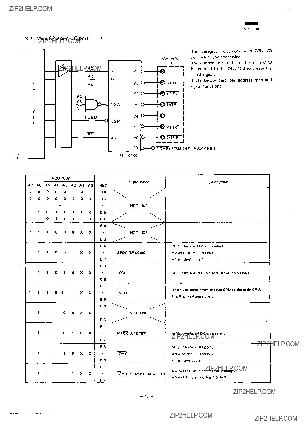
5 O IOABCMEMORY MAPPER)
SFD interface FDC chip select.
AO used for RD and WR.
A1 is "don't care".
SFD interface I/O port and DMAC chip select.
Interrupt signal from the
F 7
MFD interface I/O port.
AO used for RD and WR.
AT is "don't care".
I/O port select in the memory mapper. AO and A1 used during ~W5. WR.

MZ3500
Shown at the left is the circuit used by the CPU to select the I/O ports The out put address from the sub CPU is decoded by the 74LS138to create the select signal. Shown below is the address map and select signals.
AS 7654 M??X\
0000
0001
0010
0011
0100
0101
0110
0111
1000
1001
1010
1011
1100
1101
1110
1111
74LS138
NOT USE
- 18-

1) Block diagram
INTB
WAIT
TIMING
WAITB GENERATOR
CLK
MZ3500
Memory mapping logic
A 15
AU
INTERRUPT
PRIORITY
ENCORDER
1 N T F I)
- 19 -

MZ3500
2) Memory mapper (MMR)
- 20-

Polarity
Pin No.
Signal Name
32RF1B
33RF2B
34WATB
35RCMB
36ITFB
37ITOB
38IT1B
39TT2B
40MRQB
41WRB
42IT3B
43IT4B
44SEC
45GND
46Vcc
47SW1
48SW2
49AO
50RFSH
51SW3
52SW4
53GND
54FD1
55Vcc
56FD2
M 7, 3500
Interrupt input from the UPD765 FDC (Floppy Disk Controller).
IN
(Interrupt from Floppy)
Interrupt input from the
IN
(Interrupt from No. 0)
Interrupt input from slot 1 or 2.
IN
(Interrupt from No. 1, 2)
Memory request signal from the main CPU.
IN
(Memory Request)
Write signal from the main CPU.
IN
(Write)
Interrupt input from slot 3 or 4.
IN
(Interrupt from No. 3, 4)
Input from the FDD (Floppy Disk Drive) assignment dip switch (A), No. 1.
IN 'See the dip switch description, provided separately. (Section)
IN Ground
Input from Thesvstem assignment dip switch,
IN
"See the dip switch description, provided separately.
Mam CPU address bus
IN
Used rn the I/O port select logic in the MMR to designate device number.
Refresh signal from the main CPU.
IN
(Refresh)
Input from the system assignment dip switch.
IN
???See the dip switch description, provided separately.
IN Ground
Input from the system assignment dip switch.
IN
'See the dip switch description, provided separately.
Input from the FDD assignment dip switch (A), No. 2.
IN
*See the dip swi'ch description, provided separately.

- 22 -

M 7.3500
MAIN CPU
I/O PORT IN MEMORY MAPPER
ADDKKSS
A7 A6 A5|A4|A3|A2|Al|AO H E X UHUS 1 O
01
r\i IT
DO
D7
1 1 1 1 1 1 0 KI)1 Dl
DO 1)7 D6 D5
D4 OUT
D2
Dl
1 1 1 1 1 1 1 0 FE DO D4 D3
D2 INI
Dl
DO
D7
D6
D5
1 1 1 1 1 1 1 1 FF 1)4 I N
D3
D2
Dl
DO
D7
D6
SKQB
1 1
SKI S
M S ]
M S O
M<\3
MA2
M A I
M A O
MO2
M O I
MOO
S W 4
b??3
M\2
Sttl
she
FD3
FD2
H>1
SKDY
SACK
1 N P 2
I MM
IN'1'0
M F 2
Mhl
SRQ Bus request from the mam CPU to the
Memory system define
Bank select signal to memory area of
_J
Bank select signal to memory area of
System assign switch
1.All output signals are reset to low level upon power on, except for SRBQ that goes high.
2.Noted with a star mark "??" are input/output signals, and rest of others are processedin the LSI.
#1 I/O port output of ME1 and ME2 uses the memory at the addresses.
(
I
Mm i i
"fJ~
11 1 H
" I "
H j H
M II TO t MOI??m
n (iHj 1I 1 H M 2hTisn 1 T4h TvfT J i\=TjTNT7 JM3
1 j X X
H 1 H | 1
H j H j H
H j H j H | H
01 iri T hkoM fMont
1 h
When ME1 and ME2 are in high state. RSAB (RASA) is inhibited during memory addresses in
Wait timing generator
WAIT is issued once per main CPU fetch cycle. Its outut is tri state
MZ3500
To main CPU
1)
As ROM IPL turns to low level after power on address bus buffers (LS244, LS367) and data bus buffer (LS245) are enabled. S of the data selector 1C (LS157) is set to a low level to enable input
2)
When RAM COM is low, SRES high, and SACK low, the select input S of the selector 1C (LS157) is in low state so that input
3)
Normally, the select signal S of the selector is pulled up to Vcc level that inputs
4)
Y1 of the LS139 changes to low level when AS13 is high and AS14 and AS15 are low. In other words, the input 4B of the LS157 is at low level which brings the output Y4 to low level, so that CSof the
If SMRQ, SRD or SMRQ, SWR is in low level at this point, it enables read (OE) or write (WE). Address range, however, is 2000 to 3FFF
5)RAM (SA, SB, SC, SD) select by
SMRQ, SRD (Of) or SMRQ, SWR (WE) is at low level to select the
RAMSA .. ASVi, AS12, AS13, AS14, AST! (address 4000^17FF)
RAMSB .. AS11, AST2, AST3, AS14, AS15 (address
RAMSC .. AS11, AS12, AS13, AS14, AS15 (address
RAMSD .. AS11, AS12, AS13, ASK, ASHi (address
- 24 -

4. CRT DISPLAY
Color designation possible for each character
Color (one frame)
Blink, revers
Programmable for each character.
640 x 200 dots, B/W (Two frames)
Color designation possible for each character
640 x 200 dots. B/W (six frames)
Color designation possible for each character Color (Two frame)
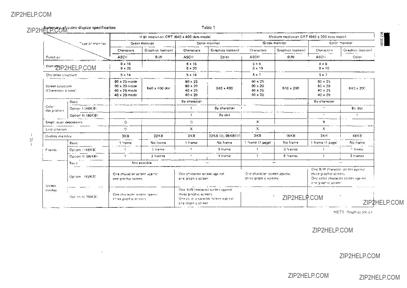
Function^^\^^
Elements
Character structure
Medium resolution CRT (640 x 200 dots mode)
Screen structure (Characters x ines)
80 x 25 mode
80 x 20 mode
640 x 400 dot
40 x 25 mode
40 x 20 mode
Color
Basic
Option 1 (48KB)
designation
Option II (96KB)
Small tetter descenders
Line creation
Display memory
O
O
3KB32KB
One character screen
One character screenagainst one graphic screen
One B/W character screen against three graphic screens
One color character screen against one graphic screen
Dip switch in the mam unit is used to select assignment of high resolution/medium resolution CRT.
Display mode must be chosen by programming.
M7 3500
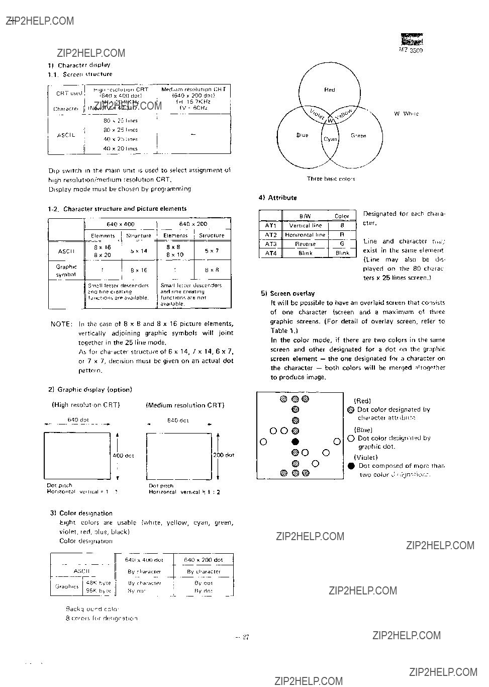
W Whne
Three basic colors
4) Attribute
B/W Color
AT1 Vertical line B
AT2 Horizontal line R
AT3 Reverse G
AT4 Blink Blink
Designated for each chaia- cter.
Line and character r,,uy exist in the same element (Line may also be dis- played on the 80 charac ters x 25 lines screen.)
NOTE: In the case of 8 x 8 and 8 x 1 6 picture elements, vertically adjoining graphic symbols will joint together in the
As for character structure of 6 x 14, 7 x 14, 6x7 , or 7 x 7, decision must be given on an actual dot pattern.
3)Color designation
Eight colors are usable (white, yellow, cyan, green, violet, red, blue, black)
Color designation
Background color
8 colors for designation
5} Screen overlay
It will be possible to have an overlaid screen that consists of one character (screen and a maximum of three graphic screens. (For detail of overlay screen, refer to Table 1.)
In the color mode, if there are two colors in the same screen and other designated for a dot on the graphic screen element ??? the one designated for a character on the character ??? both colors will be merged sltorjpther to produce image.
two color Jj>i"jrn*ion:.

MZ 3500
6)Screen overlay and displaying on two independent CRT's
As there are two video output channels it will be pos sible to display two independent screens on separate video display unit Overlay is possible on either of
screens (See preceding item 5) ) The following bit selection is needed for screen overlay
Function
Choice of outputting the character screen on CRT1 0 No 1 Yes Cho ce of outputting the character screen on CRT2 0 No 1 Yes
Choice of whether attribute or cursor be put on the frame that displayed on CRT2 (0 No 1 Yes)
Displays on CRT1 the blue elements contained in the VRAM Displays on CRT1 the red elements contained in the VRAM Displays on CRT1 the green elements contained in the VRAM Displays on CRT2 the blue elements contained in the VRAM Displays on CRT2 the red elements contained in the VRAM Displays on CRT2 the green elements contained m the VRAM
[ Choice of background color display
Color mode
Border color mode in effect
Defines the data size for the graphic RAM (0 8 bits, 1 16 bits) Defines display digits for the character screen
(0 40 digits 1 80 digits)
Connection of a 400 raster CRT
Connection of the 96K bytes VRAM
Connection of graphio GDC
25 lines/20 lines switching (0 25 lines, 1 20 lines)
NOTE Both CRT1 and CRT2 must be high resolution CRT's (640 x 400) or medium resolution CRT's 'RO x Output to each CRT may be possible in the following combination .
Output to each CRT may be possible in the following
CH
(.1-
C H + G I

7)ASCII CG
Uses an 8KB MROM contains two patterns'
640 x 400 dots ( 8 x 1 6 dots) and 640 x 200 dots (8x8 dots)
MZ3500
With 8 x 8 dot format
two kinds of patterns coexist Refer to ROM address and data code on separate information
#1 FFF
Model 3500
8 x 16 dot pattern
(4K byte)With
letter (h i j) descenders
#1 000
12
1 5 2
IASCD/JIS]
8
Without line
[Graphic symbol
'With line
HL On 16th line
VL Line ot the right of element
In the case of graphic symbol display
Both HL and VLare overlaid to the pattern
- 29 -

MZ3500
2) 20 line display mode
2) 20 line display mode
8
20
Without line
10
\\NS\\\\Mi
ASCII
20
With line
HL On 18th raster
VL Line to the right of element
e VL does not join
a In the case of graphic symbol display, VL is overlaid to the pattern
Graphic symbol
j I Graphic symbol
9)Cursor
Sharp of the cursor: Same as seen in Model 3200 Reverse and blink)
10)Light pen input
Incorporates the light pen input connector and its inter- face. The light pen, however, is an option.
Accuracy: By each character
Function: Coordinates/charactercode
11)Difference in specification with that of Model 3200
(1)There are two modes for the Model 3200; normal mode ( 6 x 9 elements) and graphic mode ( 6 x 8 ele- ments). In the normal mode of
1) Structure of VRAM
GDC1 (for character)
GDC2 (for graphic)
#BFFF
16Kh,t 1 6 K b i t
(2)No line will be displayed for the medium resolution CRT (640x200 dot).
It is possible to display line on the high resolution CRT, compatible to line the utilizing program of the Model 3200
ts-
- 30-
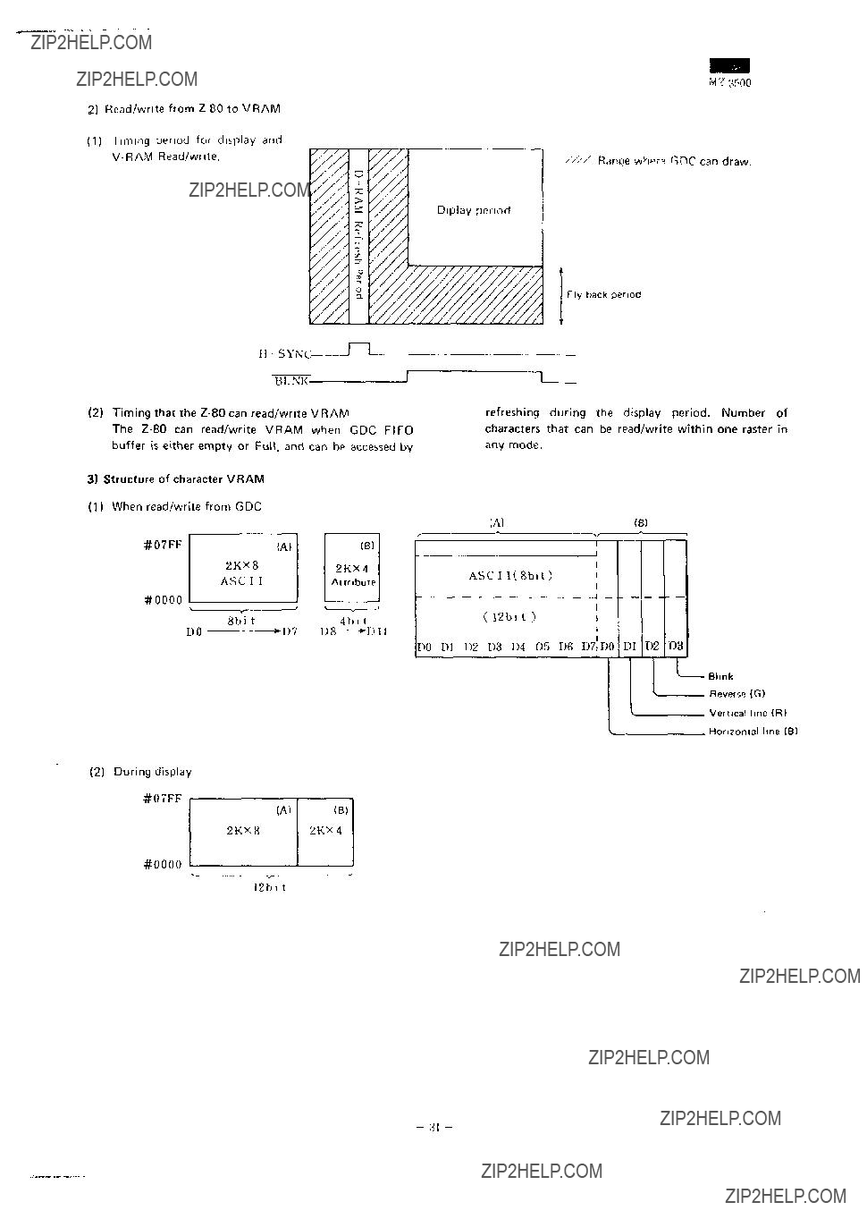
2) Read/write from Z 80 to VRAM
(1)Timing period for display and
M 7 3500
H ??? SYNC-
BLNK-
(2)Timing that the
3)Structure of character VRAM
(1)When read/write from GDC
#07FF(A)
2KX8
ASC I I
J
GDC FIFO accessed by
Fly back period
refreshing during the display period. Number of characters that can be read/write within one raster in any mode.
(A)(B)
ASCI I ( 8 b i t )
#0000
??? Blink
Reverse (G)
Vertical line (R)
. Horizontal line (B)
(2) During display
#07FF
(A)( B )
2KX8 2KX4
#0000
12bi t

MZ3500
4)Graphic VRAM memory (MZIR03)
??? Block Diagram
1.read/write Mode
The select signal RASA, RASB and RASC are generate from RAS, A14 and A1 5 which is signal of
The address is allocated to each area selected by above signal.
Read/write by
(1) 640 x 200 dots display mode
Low High byte byte
+ 8000
#4000
A
B R 16K
#0000i
2.Display mode
A14 and A15 are not valid and RASA, RASB, RASC are selected together. By the DBIN signal from
The signal of 08/16 select, after
(08/16 select: 08 for 200 rasters. 16 for 400 rasters)
During displaying
B/W: 3 frames
Color: 1 frame
#3FFF
16K
# 0 0 0 0
8bit 8bit 31,L
16bit- 32-

#3FFF
# 4 0 0 0
#0000
16K
# 0 0 0 0
16bit
5)Synchronize signal timing
(1)For 640 x 200 dots display mode
16K
16bit 16bit 16bit
Total rasters: 261 rasters
MZ3500
(2) 640 x 400 bits display mode
fH = 20.92 kHz
Total rasters: 441 rasters
Display rasters 400 rasters
(3)CRT synchronizing signal specification (400 raster
CRT)
1.Horizontal synchronization frequency (fH): 20.92kHz
2.Vercial synchronization frequency (fV): 47.3Hz
3.Total rasters: 441 rasters
4.Rasters used: 400 rasters
5.Display dots: 640 x 400 dots
6.Dot clock: (19.66MHz)
7.Timing
9.HS, VS, and VIDEO signals are supplied from the LS type TTL 1C(totem pole)
6)Setup of GCD master/slave
(1)Master/slave setup by combination
400 rasters
Master should be setup in the abovei.ia.
(2) I/O signal switching
PIT A ft to
(8255.PB7 )
VFP: 11 rasters (0.5ms)
(CSP - 2)
VSYNC
Switching
Circuit
VS- 5 rasters (0.24ms)
!VBP- 25 rasters (1.2ms)
8.Output method HS, VS. and VIDEO are indpendent outputs.

7) Graphic
Relation between VRAM address and screen (640 x 200 dots)
bOb\ir ???
CRTC block diagram
Color graphic VRAM PWB (option)

MZ3500
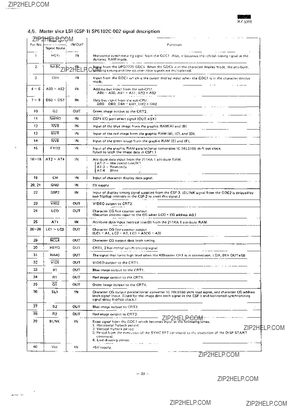
4/6. Master slice LSI
Priority
Signal Name
1 HSYi IN
2 NABC IN
3 CSR IN
4 - 6 ASO - AS2 IN
7 - 9 DSO - DS2 IN
10 G2 OUT
11 NWRO IN
12 NVB IN
13 NVR IN
14 NVB IN
15 FYD2 IN
19 CH IN
20.21 GND IN
22 DSP2 IN
23 VID2 OUT
24 LCD OUT
25 AT1 IN
29 NCL4 OUT
30 HSYO OUT
31 RA40 OUT
32 VIDI OUT
33 B1 OUT
34 R1 OUT
35 Of OUT
36 SL1 IN
37 B2 OUT
38 R2 OUT
39 BLNK IN
40 Vcc IN
Horizontal synchronizing signal from the GDC1 Also, it becomes the refresh timing signal in the dynamic RAM mode.
Input from the UPD7220 GDC1. When the GDC1 is in the character display mode, the attribute, blinking timing and line counter ciear signals are multiplexed.
Input from the GDC1 which is the cursor display input when the GDC1 is in the character display mode.
Address bus input from the
ABO = ASO, AB1 = AS1 , AB2 = AS2
Data bus input from the
DBO = DBO, DB1 = DB1 , DB2 = DB2
Green image output to the CRT2.
CSP1 I/O port select signal (OUT #5X)
Input of the blue image from the graphic RAM(A) and (B).
Input of the red image from the graphic RAM (B), (C), and (D).
Input of the green image from the graphic RAM (E) and (F).
Input of the graphic RAM parallel/serial conversion 1C 74LS166 shift out clock. (Used to latch the image data in CSP1 .)
Attribute data input from the
Input of character display data signal.
0V supply
Input of display timing signal supplied from the
VIDEO output to CRT2.
Character CG line counter output.
(Becomes address input to the CG when LCD = CG address AO.)
Attribute data input (vertical line/B) from the
Character CG line counter output.
(LC1 = A1, LC2 = A2, LC3 = A3CG = A3)
Character CG output data latch timing.
CRT1 , 2 horizontal synchronizing signal
The signal that turns high level when the
VIDEO output to the CRT1 .
Blue image output to the CRT1.
Red image output to the CRT1.
Green image output to the CRT1.
Character CG output parallel/serial converter 1C 74LS166 shift load signal, and character CG address latch signal input. (Used for the image data latch signal in the
Blue image output to CRT2.
Red image output to CRT2.
Erase signal from the GDC1 which becomes input at the following times.
1.Horizontal flyback period
2.Vertical flyback period
3.Period from the execution of the SYNC SET command to the execution of the DISP START command.
4.Line drawing period
+5V supply.
- 39 -
MZ3500
ASO
AS1
AS2
MkRO
DSO '
DS1
I)S2
HSYI
NABC
SL1
FYD2
BLNK
,r??T ,
K \ 400
I
'
hI1 rn H 1
DSP2
ATI
AT 2
ATS
AT 4
CSR
CH
5-
HSYO
NVB
NVR
D ???
F/F
J?^"
s
s ^ ' S ''
'"'
X
>- V I D 1
>
*??? ~*^
3>- V1D2
y-
???>-
CSH-
- 40-

MZ3500
46.LSI
Polarity
Horizontal synchronizing signal from GDC2 which also becomes the refresh tirniny . i j r . s ' i in the dynamic RAM mode.
Erase signal input from the GDC2 which is supplied 4T the following times:
1.Horizotal flyback period.
2.Vertical flyback period.
3.Period from the execution of the SYNC SET command to
4.Line drawing period.
WRITE ENABLE output for the graphic dynamic RAM.
Input of the display output signals (AD14, AD1 5) from GDC2. (Used to create
Input from the GDC2 by which the image memory output is sent on the data bus. (Used to create
Input from the GDC1 by which the image memory output is sent on the data bus. (Used to create BUSG, SOE, SWE in the
Gate signal of the bidirection bus buffer (LS245) which is used to read/write attribute, and character, data from the static RAM (21
OUTPUT ENABLE for character static RAM (61
WRITE ENABLE for attribute, character static RAM.
Memory control signal RAS from GDC1. (Used to create CGOE, SL1 in
Memory control signal RAS from CDC3.
(Used to create SL2, LOAD,
Address bus input from the
Chip select (OUT#5X) of the I/O port in
Data bus input from the
The signal that goes to high level (input from
Clock input from the clock generator (39.32MHz, for
0V supply
Graphic DRAM output parallel/serial converter 1C 74LS166 shift load signal.
Graphic DRAM (A), (B) RAS signal.
Double character clock output. In the character display mode, a single phase clock of the half the one character wide frequency is supplied. In the graphic display mode, a single phase clock of 8/16 dot frequency is supplied to GDC2.
Graphic DRAM output parallel/serial converter 1C 74LS166 load timing clock.
+5V supply.
Graphic DRAM output parallel/serial converter 1C 74LS166 shift out clock.
Double character clock output same as 2CK2. In the character display mode, a single phase clock of one half the one character wide frequency is supplied to GDC1 .
Character CG output parallel/serial converter 1C74LS166 shift out clock.
Character CG output parallel/serial converter 1C LS166 shift load signal.
Character CG address.
Character CG output enable signal.
Timing signal by which the graphic DRAM output is sent on the data bus.
Graphic DRAM RAS (ROW ADDRESS SELECT) signal
- 41 -

M/3r>00
CSP 2 Block Diagram
t f
^??? Bl SC,
D- SOf
O- SHE
^
- 42 -

M 7.3500
1
2
3
4
5
6
7
8
9
10
11
12~19
20
21
???Since the image drawing process is automatically interrupted in the dynamic RAM mode the refresh address is output during the HSYNC period. It can also be used as the refresh timing signal.
???Refresh is accomplished by suppressing the CAS signal derived from the RAS signal in the external
circuit when the HSYC is at h gh lebel (Horizontal Synchronous - Refresh timing)
2.When the slave is operational : The synchronizing signal generationcounter is initialized by a high level input.
(Address/Data bus 0- 12)

-

4 8 CG Address Select Circuit
I
==
0020
8 b ts
M "
When 200 rasters on ASCII in use
(only the high order 8 bytes of 16 bytes are set to low level I
ASCII character structure of the 200 raster CRT
ASCII characterstructure of the 400 raster CRT
[Circuit description] (Purpose)
The character genrerator (CG) incorporates all character code^ used by the 200 raster video display unit of the \X 3500 and by the 400 raster video display unit of the \X 3500 The CG address select cirruit is therefore used to select those modes
[Operational description]
1When the 400 raster CRT is in use, RA40 is set to high level which sets A12 of the CG to high level at all times, so that the CG address above 1000 is selected Also, gate (1) opened so that LC3 is input to A3 of the CG At the same time, gate (3) is opened so that the gate of the LS240 is closed every 16 bytes
2When the 200 raster CRT is in use, RA40 is set turned to low level which sets A12 of the CG to low level continuously, so that the CG address 0000 OFFF is selected Also, gate (2) is opened so that the
CPU
- 45-
MZ 3500
0 40 Digit
From1 80 Digu
(8255 PB7) CH48
80 digit, 16bit/word Master is
[Circuit description]
When more than two UPD7220 GDC's areto be operated in parallel, one must be assigned to the master and the other to the slave in order to mantain synchronous display timing. The master and the slave are determined according to the table below. The above circuit shoud be used to compare with the table description.
The master GDC must be set as indicated above.
[Oprational example]
If it was set to 80 digit, 16 bit/word mode SRES will be 0 when CH48 = 1, 0816 = 1 when not in the reset condi- tion. These signals are supplied to terminal A (weight 1), B (weight 2), and G (gate), and set terminal Y3 of the decoder 1C LS139 to "0", so that the YSYNC output of the GDC2 is input to terminal EX SYNC of the GDC2.
SRES (From MMR)
40 digit. 16bu/word
80 digit, 8bit/word Master is GDC
40 digit, Sbit'word Master is GDC 1
- 46-

BL'SC
BLNK Erase signal
TTJ Period that the GDC is enabled to read/write and draw graphic data.
BLANK
[Circuit description]
With respect to GCD1, the assignment during read/write
of the character
character VRAM select circuit is provided. Jo accomplish this function.
8bil
- 47 -

MZ3500
Read/write of the Model 3500
NO
YES
Set GDC command code
YES
Set parameter for the command
(1)Read/write via the 16 byte FIFO.
(2)Read/write of
(Outline of the read/write data via the FIFO;
Method used to give a command to the GDC.
YES
Set parameter for the command.
I
Command must be given to the GDC in the same manner. On next page is the program of the above flowchart.
- 48-

MZ3500
(Subroutine lo send command and parameter to the GDC via the FIFO)
HL reg ??? First address of the command code oarametpr
B. reg ??? Q'ty of data.
C reg - 60H (graphic GDC), 70H (characterGDC)
> FIFO Empty?
;
;Return if parameter not sent.
f FIFO Empty?
;PARAMETER ??? GDC
;Return when all parameters were sent.
RET
Example of graphic drawing by GDC
1) Dot display
VRAM
structure
Example to display a dot on the fourth bit of the address
CSRW C 49H
P1 01H ??? Low order one byte of the ab- solute address
P2 OOH ??? High order one byte of thp ah solute address
P3 30H - Dotaddress (dAD)
WRITE C 23H - COMMAND CODE
VECTE C 6CH - COMMAND CODE
- 49-

the dot address. Set the command code of the SET mode (set mode plus CLEAR, REPLACE, and COMPLEMENT modes using "WRITE", and specify to start with
5000 ??? 49 H
5001 ??? 01 H
5002 ??? 00 H
5003 ??? 30 H
CSRWdata
5004 ??? 23 H } W R I T E data 5005 ??? 6CH } VECTE data
C
HL - Topaddress of theCSRW data
Command, parameter of CSRW - GDC
B - Byte size of the WRITE data HL - Topaddress of theWRITE data
Command, parameter of W R I T E - GDC
B ??? Byte number of the VECTE data HL - Topaddress of theVECTE data

M 7. 3500
2) Straight line drawing
VRAM 16 bit structure
Example to draw a straight line from (X, Y) = (3, 1) to (X,
Y)= (635, 1).
Coordinates must be changed to absolute addresses. (3, 1) - absolute address = 0028H
Dot address = 2H
Displacement between two points when the line draw direction is OA (to the right): X =
Y=0
Whereas.
CSRW C 49H PI 28H P2 OOH P3 20H
TEXTW C 78H
PI FF
P2 FF
VECTW C 4 CH
PI OAH
P2 78H
P3 0 2 H
P4 88H
P5 H>H
P6 1 OH
P7 FBH
P8 O O H
P9 O O H
W R I T E C 23H
VECTE C 6CH
HAD I, ,H
dAU
Kind of line (solid line)
} Drawing direction
}
\1 AX I
1
[Explanation]
Specify the kind of line by TEXTW, using C for command code and P for parameter, and specify the line drawing direction using VECTW and above four values using X and Y. The rest will be same the dot display It is also possible to display a dot using the line drawing method for any line drawing direction using X = Y = 0.
M Z 3500
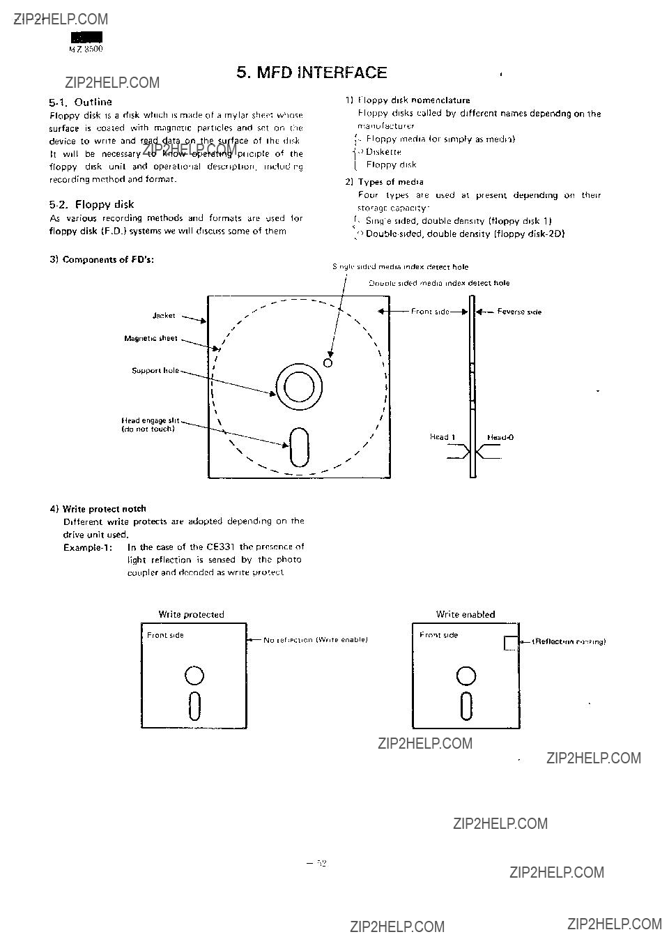
5. MFD INTERFACE
Floppy disk is a disk which is made of a mylar sheet whose surface is coated with magnetic particles and set on the device to write and read data on the surface of the disk It will be necessary to know operating pnciple of the floppy disk unit and operational description, including recording method and format.
As various recording methods and formats are used for floppy disk (F.D.) systems we will discuss some of them
3) Components of FD's:
1) Floppy disk nomenclature
Floppy disks called by different names dependng on the manufacturer
[>- Floppy media (or simply as medn) <???' Diskette
Floppy disk
2) Types of media
Four types are used at present depending on their storage capacity
(>- Single sided, double density (floppy
[??
Single sided media index detect hole
Double sided media index detect hole
Head engage slit (do not touch)
4) Write protect notch
Different write protects are adopted depending on the drive unit used.
Write enabled
Front side
- (Reflect"n<! r??ywing)

Two types of write protection are used and attention must bepaid to the presience of the label because it may cause a wrong result if the label is used improperly.
5)Media recording methods
Two recording methode are used:
???FM method (Single density)
This method is called the freqency modulation (FM)
n 1 n n 0
C D C D C
or double frequency (DF). Clock and data are written on the media which requires that a clock bit that precede the data.
(C: clock, D: data)
Waveforms of data written or read in the FM mode are shown below.
r*-
Write current: The write data is input to the flipflop and is inverted each time a pulse is received to change the direction of writing current.
Read waveform: The peak of the waveform is detected at a change of magnetic flux. The waveform is than shaped to obtain read data identic it >.<_??? tlirf write data. Data cycle will be 4/^s.

MZ3500
o MFM method (double density)
The MFM method writes data on the basis of the condi tion metntioned below, and it yields a data density two
times the data density of the MFM mode (The unneceb sary clock pulse is eliminated using this method ) (Condition) Clock is written only when there is no data
The clock pulse (Ci will be eliminated in above illustra tion as there is no data preceding or following the clock Because the data rate is 2/Js for this method, it is possible to obtain twice the density of the FM method
6)Media recording format
Media is formatted according to the IBM format
For Double side media, data is written on the front side
NOTE Three types of write data cycl??- (2f ~>t"> SA*S) are used The read/write waveform is identical
to FM method
Floppy disk
Tracks, consists of 40 tracks,
Sector.
Recording density: 256 bytes/sector

M 7 3500
Shown below is an enlarged view of data format
sequence Writing starts as soon as the index hole comes
through the index detect hole
DATADATA I UI I ) DA I A
<[ t
I N D E X
\M
Start point
Hatched portion is a recording gap
I D
AM TT HH SS DL CRC CRC
ID section CRC check code
Size of data section
(00) H ??? 128 bytes
(01) H ??? 256 bytes
Sector number
Head number
(00) H
(01) H
??? Track number
??? ID address mark which begins the ID section
7)Formatting
To write the above format (ID section, data section, gap) on an entire surface of a new floppy disk is called formatting
Note 1 Formatting may also be called initialization. The word "initialize" is also used as a software term to clear the data section or to partition data area. Keep the difference between formatting and initializing in mind.
Note 2 Unless formatting has been done on a properly adjusted floppy disk drive unit, an erroe may occur on another floppy disk drive unit
8)Data write procedure
Described next is the procedure to write data on the FD.
(1)The head is moved over the track to be written.
(2)The head is loaded
(3)ID section is read and repeated until the desired section is reached
(4)When the desired ID section is found, data is written on that area (DATA AM is also written )
(5)The data thus written is now checked if it was written correctly (read after write) The respective ID section is read while the media makes a full turn
51
DATA
AM DATA CRC CRC
'Data address mark
(or delete address mark)
NOTE The delete address mark
is written to indicate invalid data It is often written on
a new floppy disk as there are no valid data on it
(6)The sector of the identical ID is read and verified with the write data Because of thr pad dftei Ar.'e capability the possibility of an error in the written data is quite low
9)Data read procedure
Described next is the procedure to read data from the FD.
(1)The head is moved over the track tu
(2)The head is loaded
(3)The ID section is read and repeated until the desired sector is reached
(4)When the identical IDsection is found, the
MZ3500
> MOTOT ON
- 56 -

M 2 3500
FDC (UPD765)
WE : Write Enable
- 57 -

MZ3500
UPD765 signal description
Function
+5V
Single phase, TTL level clock
Set the FDC into an idle state, and all drive unit interface outputs, except PSO, 1 , and WDATA (don't care), are set to low level In addition, INT and DRW outputs are set to low level DB goes into an input state.
Validates RD and WR signals
Bidirectional,
Control signal to write data to the FDC via the data bus
Control signal to read data from the FDC via the data bus
The signal used to indicate a service request from the FDC It is issued at every byte in the non- DMA mode, or upon completion execution of a command in the DMA mode
The signal used to select the status register or data register of the FDC for access via the data bus. When 0, it selects the status register When 1. it selects the data register.
FDC to memory data transfer request signal in the DMA mode
The signal that indicates use of the DMA cycle During the DMA cycle, it functions identically toCS.
Drive unit select signal, with which up to four drive units can be selected.
The signal used to designate the operation mode of the VFO circuit When 0, the MFM mode is assigned. When 1, the FM mode is assigned
The signal used to designate the operation mode of the VFO circuit When 1, it permits reading operation. When 0, it prohibits reading operation
Signal used to discriminate the read/write signal from the seek signal that used for drive unit interfacing signal. When 0, it indicates RW When 1 , it indicates
Signal used to load the read/write head
Signal used to select head #0 and head #1 for the
When the RW/seek signal is operating as RW, the signal works as LCT which indicates that the read/write head is selecting the cylinder above 43. When the RW/SEEK is operating as SEEK, it works as DIR which indicate seek direction When 0. seek is made towards outer side
When 1, seek is made towards inner side
When the RW/SEEK signal functions as RW, it works as F LTR which resets any fault condition as the seek step signal.
Signal used to indicate that the drive unit is ready for operation
When the RW/SEEK signal is operating as RW, it function as WPRT which indicates that the drive unit or the floppy disk is write protected. When the RW/SEEK is function as the SEEK signal produces 2 SIDE which indicates that a double sided media is in use.
Signal to indicate the physical start point of the track.
When the RW/SEEK signal is operating as RW. it works as FLT which indicates that the drive unit is in a fault condition. When the RW/SEEK is operating as SEEK, it works as TRKO which indicates that the read/write head is on cylinder 0.
Signal used to indicate the termination of a read or write operation
Data written on the floppy disk consists of clock bits and data bits
Signal to indicate write enable to the drive unit
Data write timing signal which is 250kHz in the FM mode or 500kHz in the MFM mode
- 58-

22WINDOW
'
MZ350C
Function
Signal used to either advance or delay the write data in writi ng under the MFM mode, to obtain tir rung adjustment for reading. The WDATA signal is controlled as shown in the table be ow
Read data from the drive unit consists of clock bits and data bits.
Signal created in the VFO circuit which is used to sample RDATA. Phase syncroni^i carried out in the FDC for RDATA data bits and WINDOW.
There are two ways of recording data; FM recording method and MFM recording method.
2)MFM recording method
(1)Data bit is placed in a middle of a bit cell.
(2)When the data bit is "0", a clock bit is placed before the current bit cell. (See Fig. 1)
1) MF recording method
(1)Clock bit indicates a bit cell.
(2)Data bit is placed in a middle of a bit cell. (See Fig. I.
As seen from the above illustration, bit density of the MFM recording method is twice the FM recording method. In other words, data density of the MFM recording method doubles that of the FM recording method. For the
Model 3500, only side 0 of track 0 (128 bytes/sector) is written in the FM mode and rest of other tracks are recorded in the MFM mode.
I/O port used in the MFD interface is as follows.
D7
D6
D5
D4
OUT
D3
1)1
DO
U2
Dl IN
DO
DACK
ME
SCTRL
TC
TRIG SEL3
SKI. 2 SEL1
SELO
M . ON
INDEX
DRQ
Used for data transfer between the CPU and the FDC.
INT from the FDC is output enabled on INTFD. FDD select signal output is enabled.
TC to FDC.
Trigger (motor on) of the timer (555) Selects FDD 3
Selects FDD 2
Selects FDD 1
Selects F D D O
ON/OFF state of the motor
INDEX signal from the motor
DRO from the FDC.
- 59-

M 7.3500
Set the counter to 200ms.
(Actually, slightly longer than 200ms.)
K K I T E DATA
(Fig. 2)
(Table!)
WDATA-
8MHz
CLOCK
EARLY-
NOMAL-
LATE-
(Fig.3)
The precompensate circuit is used to compensate the peak shift before writing.
The FDC sends out the compensation rate to PSO and PS1 and the data bit location is shifted according to this signal. With issuance of WDATA. the value dependent on PSO and PS1 is set in the LS163. (See Table 1.) For instance, when both PSO and PS1 are low, it will set "1101 (D)" to the LS163, counted up by the 8MHz clock, and QB is sent out When it becomes "1110, 1111". When in EARLY (PSO= "H", PS1="L"), the value "1110(E)" will be set to the LS163 so that the output is issued 125ns earier than "not changed". The QB output, however, will be supplied for a period of two clock cycles.
Above operations are all controlled via the FDC. 1) Control during read and write
I
2) Control during seek and recalibration
SEEK (or RECALB) command to FDC
I
HALT
(waits for interrupt) Read'result status from FDC.
Insertion of a media on the MFD is detected via the signal
INDEX from the MFD. Since it takes 200ms for the media
to make a full turn, "NO MEDIA" is detected signaltNI)R t T K Y INDEX does not appear within 200ms.
- 60 -

In the case of the MFM method, need to trace cycle fluc- tuation is further increased, as a peak shift is apt to occur because there are three write data cycles.
(Peak shift). Data read cycles fluctuate as the flux change point is moved forwards or backwards.
{VFO circuit): Variable frequency oscillator
6.0 40 20 0 20 40 60
( a )
When the output waveform is observed after writing a single pluse on the floppy disk, the waveform show in (a) appears. Shown in (b) is two pluses of 4jis interval.
1) Purpose
String of data
pulses from the FDD.
Data window
String of separate data
MZ 3500
Write pulse
Polarity inversion
Read waveform
Regenerated pulse H
C b )
Polarity inversion
(c)
Deviation in the peak point is called peak shift. Since pluse intervals of the MFD in actual operation are 4ns, 6/JS, and 8/^s, the largest shift takes place when a pluse appears 8/Js before or after 4/JS,as shown in (c).
n n
Data from the clock or data portion must be differentiated when read from the FDD. For this purpose a window pulse is used. In order to increase read tolerance, the VFO circuit carses the window to trace phase changes in the read data that take place during a floppy disk drive motor speed change.
- 61 -

MZ3500
2) VFO circuit configuration
Window
SEPARATED DATA
Data separator
SEPARATED CLOCK
The VFO circuit hasthe following capabilities.
(1)Two modes: MFM and FM.
(2)The VFO circuit operation is suspended during the SYNC field located before the ID field and data field.
(3)After suspention, the VFO circuit will synchronize with the read data (timing is affected by a speed change in the FDD). Fluctuations in an individual bit that may be seen (peak shift are ignored.
VFO circuit
+5V RtAD DATA

MFM Mode
AlMHz _rLTLJT_r
B)QA)
1_
Nomal
STD
Eary
n J~L
Delay
??

MZ3500
A 4M
B ( Q A )
C ( Q B )
D ( Q C )
WINDOW
E
F
L
Normal O
P
F
L
Advanced
Q
O
P
L
K
Delayed
Q
O
P
FM mode timing chart
1 1
Does not trace ?? I

2
,??? ^
UJ
s
..
5
S3
OS
UJ
H
.
^
o o O o 0 O
c o
(O
0
"c ???
CO
0
/
/
0
0
\\\\
/
/
o
-
t-
Q
-
^_t
u
TT
O
CTJ
U.
o
1
c o c o o
~
Q
0
I o
-
c-
o D o -
Q
U
00
(J
-
W
w
T??? 1
U,
CO
Q
-
to
U, U,
U- U.
a.s
5
"o s
u
ro
"O Q. J2
(U
??I 2
<u 00
????? of O "S'o
"*" 1C *"
i."6
6 O 4J
iui^
<u J: r "??
- ^J O o 2 r~ <??? >??-
02 - H h
H a
Q
CL
???
o
*#-
.2
73
QJ
O
O O
1 ?? O O
CD" ca cc
Csl m
8
?? U3
U
lO
10
UJ
0)
2
?????? , ^
?????? Reverse side
M/asoo
Track 0, sector 1 information (SBACIS) (Fig 1)
I Fail name (8 bytes) Expander Volume name
cc M A,r,Ar . .4 (3 bytes) (8 bytes) FF No ALOAD command
80 File specification only
01 With operand
Drive NO
All "F" when ALOAD command
is not on
ALOAD
Status line No label (8 bytes)
(Sbytes)
Contents of X register
When used for the line number (when line No 1 23) These three bytes are in effect
34 35 36 3b>tesfj$!l
00 01 23
When used for a label (Wight bytes are in effect a n d r e s e a r e )
343C
- 66 -

M7 350?
/
76iy 7 EH
77/ FFH
\1
Indicates the byte position
??? from the top of directory.
MAPNa
Block NO
Starting block number (directory)
- 67 -

MZ3500
oBlock number allocation
The program and data areas are located after Track 2 1 block = 2K bytes (8 sector)
I
39 B148 B149 B150 B151
2Kx 152 = 304K
Each track is blocked in the following manner:
I
38B72 B73
39B74 B75
2KX 76=152K
???Sub IOCS can bedivided into either blocks If divided to less than eight blocks, the block that follows
- 68-

MZS500
6. R232C INTERFACE
Input/output format
No of channels
Code used
Baud rate
Transmission system
Synchronization method
Communication control procedure
Data format
LSI used
1 channel
JIS
110 to 9600 bits/sec
Stop bif 1/1.5/2, with or without even or odd parity.
8251 AC
(Programmable interval Timer)
with parity
Example:
Stop bit of precedingdata
Stop bit
Parity bit Stop bit (1 or 2 bits)
,
Y
Stop bit (1 or 2 bit
Stop bit
- 7) -

MZ3500
ON
SW5 Causes an error when the ER signal is low or open during data output.
SW6 Always high when power is on to the main unit.
SW7 Causes on error when the PO signal is high during data output.
OFF
ER signal is disabled.
The CD signal is set high while data output, but would not be set high when the
Polarity is inverted.
There are two control words for the 8251AC.
(1)Mode instruction: Defining general operational para- meters, such as unit, stop bit, etc.
(2)Command instruction: Defining status words used for actual operation, such assend/receive enable, etc.
1)Definition of generation operational parameters
???Baud rate
???Character size
???Even/odd/off parity assignment
??????Stop bit size
"Corresponds to channel command of BASIC.
c START
8251AC internal reset
8251AC mode instruction
- 72 -
MZ3500
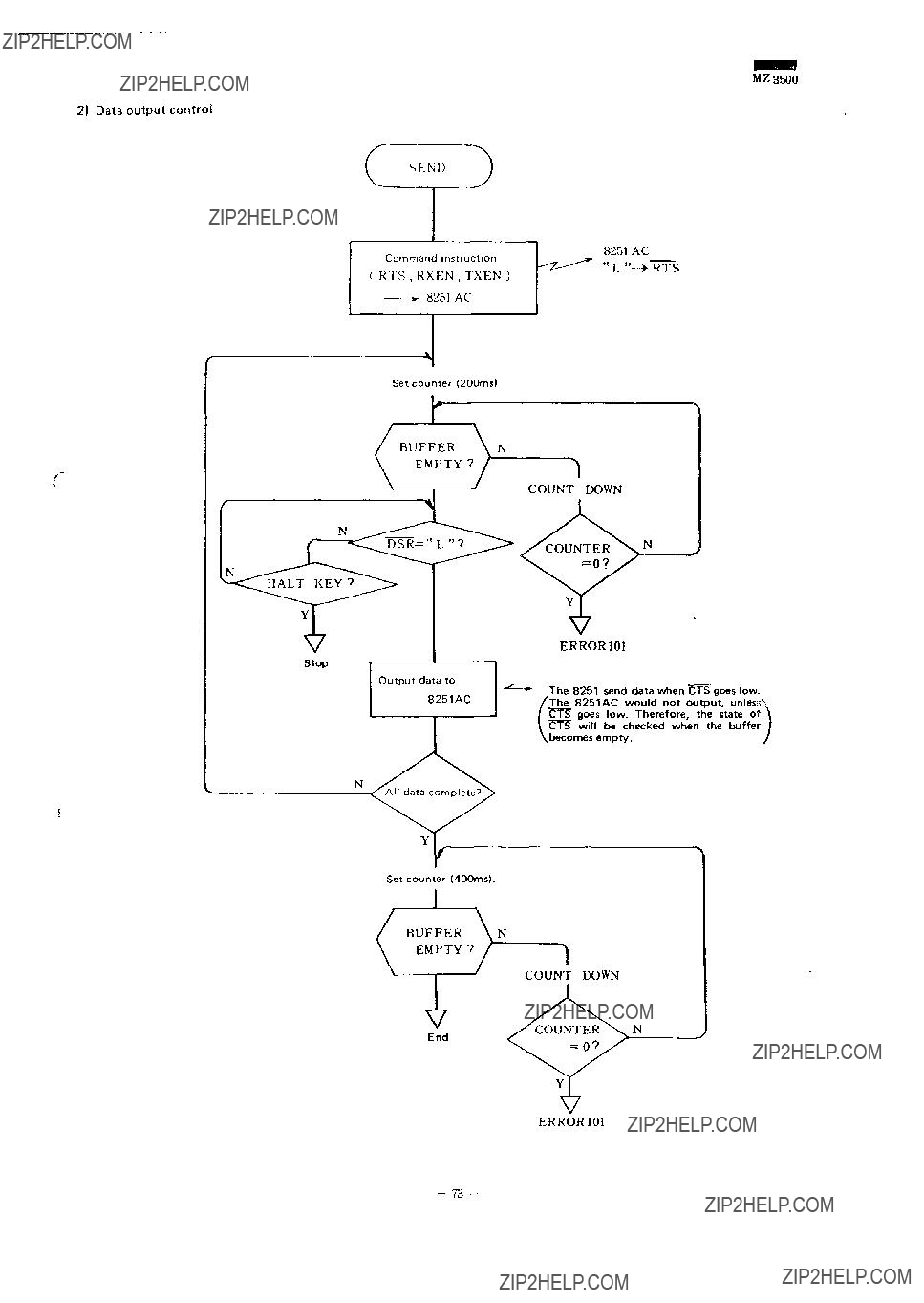
2) Data output control
S K N U
Set counter (200ms)
Stop
Output data to 8251AC
ERROR 101
The 8251 send data when CTS goes low. The 8251 AC would not output, unlessv
ERROR 101
- 73 -
M/3SOO
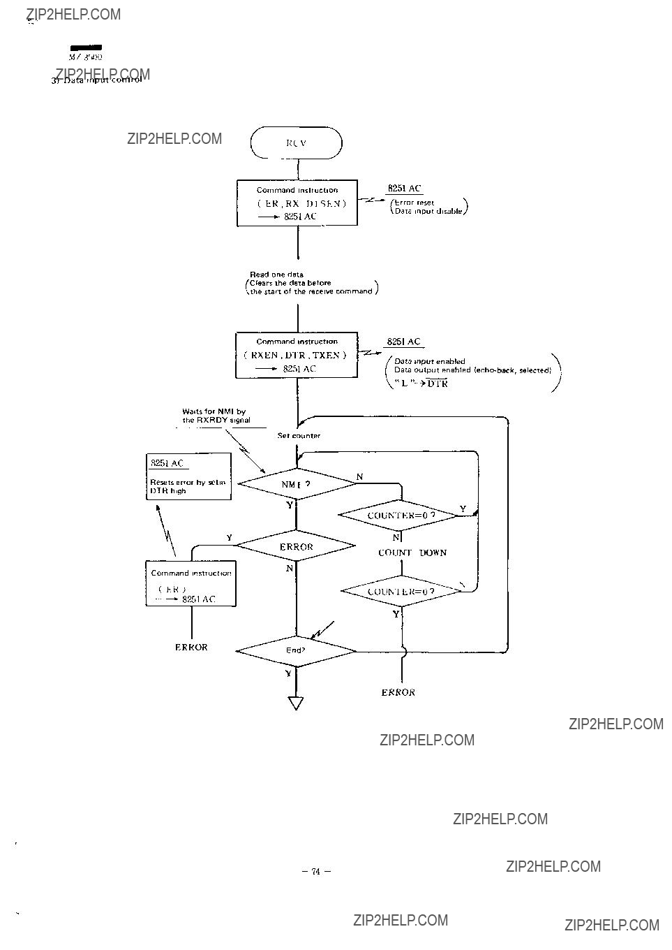
3) Data input control
R C V
\" L
Waits for NMI by the RXRDY signal
Resets error by setin
DTR high
Command instruction
( tK >
8251 AC
ERROR
ERROR
- 74 -
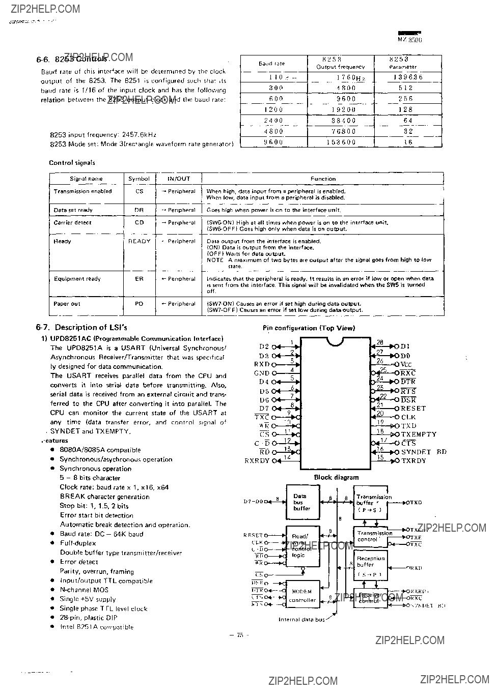
Baud rate of this interface will be determined by the clock output of the 8253. The 8251 is configured such that its baud rate is 1/16 of the input clock and has the following relation between the 8253 output clock and the baud rate:
8253 input frequency: 2457.6kHz
8253 Mode set: Mode 3(rec'angle waveform rategenerator)
Control signals
???Intel 8251A compatible
- 75 -

2)
The
Features
???
???Three sets of
???
???Programmable six operational modes and timer duration
???Choice of binary counter/BCD counter
???
???Single +5Vsupply,
???Intel
Pin configuration (Top View)
.VCC
Block diagram
- 76 -

8 2 5 1
8253
INTO TO MAIN FROM SUB
INT TO SUB FROM KEY
STK= (L)
M 2 3500
READY
CS
PO (MPER SUT), ER
CD
RD
OUT 0 of 8253
SD
To 3iil>CPU of
8253 OUT
- 77 -
PC 6
PC 7
PC 0
PC 1
PC 2
v DS6
^ DS7
*2,4,6,... 28areGND.
*Ahnwp nin numbers are of the
Function
Data is transfered to printer when STROB is high.
Data output to the printer
- 78 -

The 8255 is used for the LSI to control the parallel inter- face. The 8255 can be set in the following mode.
/PORT A: MODE 0
IPORTB: MODE 1
C:Output
74.Data transfer timing
BUSY
ACK
( 8255 A v
DATA
STROBE
( M 1 N ) l^s(MIN)
Because it is not possible to directly it uses interrupt for key processing ACK signal is latched by means of
sense the ACK signal as and RS232C input, the the OBF pin function
PRINTER:
330P, 331P, 332P
*Broken line in the above figure represents timing for the
'For detail of timing, refer to Manual provided with printer.
Set the 20 second counter.
STROBE OUT
Set the 20 second counter.
- 79 -

M / 3500
8255 ON SUB CPU BUS
I N
OUT
8255
chip address(0011/xxxxj
Group A: Mode 1
Group B: Mode 0
INPUT P O R T C 7 4 L S 2 4 4
7 4 L S 2 4 4
port address[0100/xxxx]
IN
#4X
OUT
PA7
PA6
i'A5
I'A4
I'A3
PA2
PA1
PAO
PC7
PC6
PCS
PC4
PCS
PC 2
PCI
PCO
PB7
O PB6
3
PBS
PB4
PBS
PB2
PB1
PBO
C D S 7 D
C D S 6 D
CDS5D
C D S 4 3
CDS33
C D S 2 D
cosn
C D S O D
DATA8
DATA"
DATA6
I) AT A5
C2
Clock
Cl
CO
STRB
HLT KEY
STK
Keyboard
DK J
PUTR
PE Printer
BUSY
Reads the 8255 OBF (PC7) output or timer output.
- 80-
M 2 3500
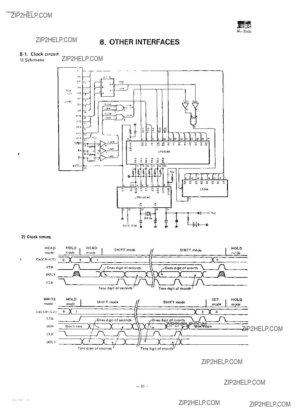
8. OTHER INTERFACES
1) Schematic
- 8) -

MZ3500
3)^PD1990AC Block diagram
OK O
Description
Holds
Data input/output
Data of the
Data in the time counter is read to the
Input/output format
Example: In the case of 10 o'clock, 25 minutes, 49 seconds, July 30th.
- 82 -

Music output waveform
??? Tonal signal OUT1
???Sustain PC4
???2SC458 emitter
???2SC458u collector
???Speaker
??GETE1 J
PD8255
mmmil
1
- 83 -

M/3500
83. Expansion and interrupt (See
2)Expansion unit
Signal assignment by slot
SFD CONTROL ???
V O I C E
DRAM control signal
32K mask ROM
B A S I C (
8K mask ROM
ROM1
ROM2
ROMS
ROM4
INT1
INT2
I NTS
INT4
L
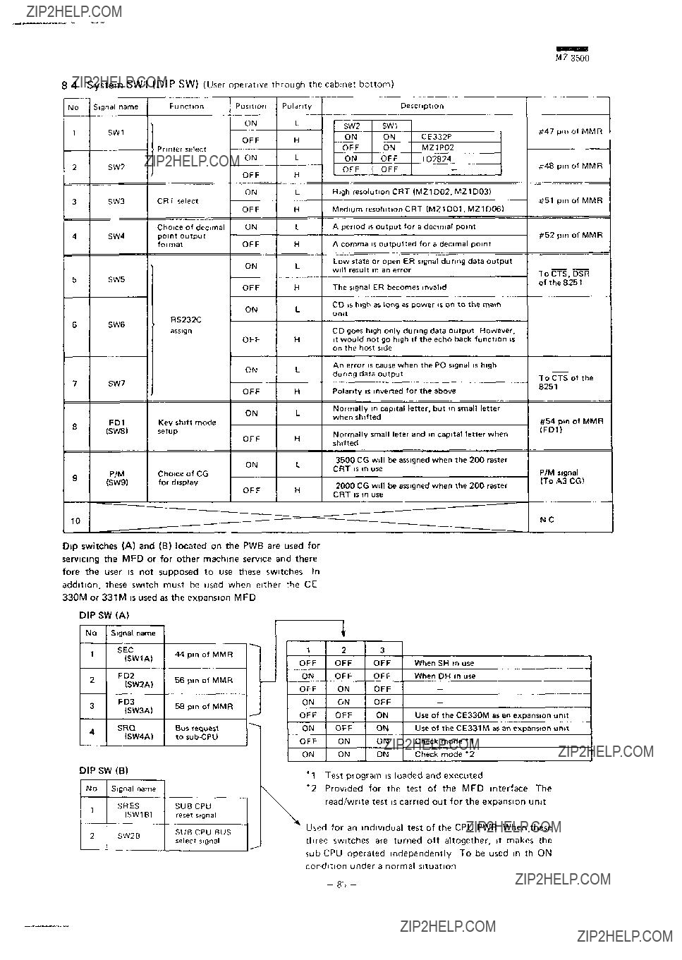
8 4 System SW1 (DIP SW) (User operative through the cabinet bottom)
M 7 3500
No
1
2
3
4
5
6
7
8
9
10
Description
SW2 SW1
ON ON CE332P
OFF ON MZ1P02
ON OFF IO2824
OFF OFF
High resolution CRT (MZ1D02. MZ1D03)
Medium resolution CRT (MZ1D01, MZ1D06)
A period is output for a decimal point
A comma is outputted for a decimal point
Low state or open ER signal during data output will result in anerror
The signal ER becomes invalid
CD is high as long as power is on to the main unit
CD goes high only during data output However, it would not go high if the echo back function is on the host side
An error is cause when the PO signal is high during data output
Polarity is inverted for the above
Normally in capital letter, but in small letter when shifted
Normally small leter and in capital letter when shifted
3500 CG will be assigned when the 200 raster CRT is in use
2000 CG will be assigned when the 200 raster CRT is in use
#47 pin of MMR
??48 pin of MMR
#51 pin of MMR
#52 pin of MMR
ToCTS, DSR
of the 8251
ToCTS of the 8251
#54 pin of MMR (FDD
P/M signal (To A3 CG)
NC
^=??? =T
Dip switches (A) and (B) located on the PWB are used for servicing the MFD or for other machine service and there fore the user is not supposed to use these switches In addition, these switch must be used when either the CE 330M or 331Mis used as the expansion MFD
DIPSW(A)
WhenSH in use
When DH in use
???
???
Use of the CE330M as an expansion unit Use of the CE331M asan expansion unit Check mode *1
Check mode *2
sub CPU operated independently To be used in th ON condition under a normal situation

X ><^ OFF OFF OFF
\(f Canbe in either state
???
Switches are set in this manner before shipment of machines this us the
Switches are set in this manner when the SH is used for the optional MFD
Switches are set in this manner when the DH is used for the optional MFD
Test mode *1
Test mode "2
Individual CPU PWB test
- 86 -

MZ3500
9, POWER CIRCUIT DESCRIPTION
1. BLOCK DIAGRAM
(Block diagram)
A. +5V and +12V supplies
1.Functions
a.Supply voltage is first rectified in the rectifier circuit and sent out to the switching regulator via the over- current detector provided in the overcurrent protect circuit.
b.Next, the voltage is converted to the +5/+12V output in the switching regulator and sent out to the noise
???Nfilter.
c. Change in the switching regulator output voltage is sensed by the control circuit and is fed back to the switching regulator after being amplified in the amplifier located in the control circuit, for maintaining the output voltage to a constant level.
d. The signal from the oscillator is supplied to the switch- ing regulator through the control circuit for driving the switching regulator.
e. For prevention of overcurrent, the protect circuit is used for stopping the oscillator when an overcurrent is met, and it makes the switching regulator to halt in order to shut off +12V/+5V supply.
2. Description of each block
a.Overcutrentprotect (control/protect) circuit
When an overcurrent is met in the +5V/+12V circuit, it causes to increase the voltage at both ends of the over- current detector resistor R1, which in turn causes to increase the Q3 collector current, for, there arises larger voltage difference between the emitter and base of the
transistor Q3. This makes the gate voltage of the thyns- tor increased owing to activation of SR. Witr, jctivation of SR it makes the oscillator voltage dropped to the GND level at the point "a" to stop oscillation, which also makes the switching regulator stopped by the de- activation of the transistor Q5 oscillation. This causes the transistor Q5 inactive, and it shuts off the +5V/
+ 12V supply,
b.Oscillation circuit
As the Q1 emitter voltage is at almost GND level whe- the transistor Q1 is active, the Q2 base voltage tem- porarily drops close to the GND level by means of C6, which in turn makes Q2 inactive and the Q2 emittei voltage increases.
Then, the Q2 base voltage comes to rise as C6 begins to be charged through R6, and the transistor Q2 starts to activate again. With activation of the transistor Q2, the Q2 emitter voltage starts to drop and the Q1 base voltage is temporarily dropped by means of C5, to shut off the transistor Ql, which causes to increase the transistor Q1 emitter voltage.
Next, as C5 is charged by R5, it makes the Q1 base voltage increased which puts the transistor Ql into activation. In this manner, transistors Q1 and O2 are alternately turned on and off to keep oscillating.
C5 and C6 are charged through R5 and R6 by on/off action of the Q1 and Q2, and discharged through Ql and
Q2.
M 7,3500
Switching regulator
(Switching regulator and constant voltage control circuit)
??VR isthe+5V or+12V adjusting VR.
???D3 isprovided to discharge current from Cj after power off.
- 88-

M23500
c. Power switching circuit
As the signal from the oscillator is amplified through Q7 to Q6 to change current to the transformer T2. it causes voltage to appear on the base of Q5 (one of components is cut by D1), so that the transistor Q5 begins to per- form switching operation in synchronization with the oscillation frequency. As Q2 is switched, current is supplied to the emitter side of the transistor Q5, which produces smoothed voltage through the capacitor C1 and the coil L2. The circuit composed of D4 and VR1 is the reference voltage for the +5 or + 12V supply, which is used to control the emitter current flowing to the transistor Q9. The current supplied from Q9 is used to create Tr3 inactive by the delayed C1 and C2 voltages which supplied from
3. Alarm circuit
(Alarm generation circuit)
When power turns off, the voltage accumulated in C1 and C2 are supplied to the base of Tr2 via Tr1 ... and D3, so that Tr2 is kept active and Tr3 inactive for some- times after power off.
Timing chart
SW
+5V
PFD

MZ3500
10. MZ1K01 KEYBOARD CONTROLLER CIRCUIT DESCRIPTION
1)Input Buffer Capacity: 64 bytes
???
???When an overflow is detected, the overflow code is affired to the
2)Rollover
???2 key rollover (exemption in the CTRL mode)
(Entry of the second key depression can be accepted even if more than one key is pressed at same time.)
???Simultaneous depression of more than three keys is ingnored.
3)Key bounce
15msec (Key spec
(Indicates unstable state as shown in Fig.
4)Key
5msec (norma), 20msec (max), 15msec (allows for key bounce)
5)DEF Key
Twenty definable keys are available in combination with the CTRL key.
[
-- -
6)Handling of functional symbols and graphic symbols See the code table.
7)Useof the CTRL key to discriminate RUN and CONT of the DEB key.
Push the DEB in conjunction with the CTRL key to start running.
8)Handling of special codes
COPY command: CTRL | 1 J (ten key) ESCape CTRL
BRKCTRL
9)PRO/OP
Sent to the CPU after power on and when PRO/OP is changed.
10)HOME key
CTRL [ HOME] Returns home after clearing the display screen.
[HOME] Only the cursor returns home.
12) Mode indication on LED
13)REP
Key repetition will take place when a key depressed for more than 0.64second. Entry of other keys is permitted during key repetition. When two keys are depresssd at the same time, an alternate key entry will not be accepted. This rule does not apply to simultaneous depression of more than three keys.
- 90 -

MZS500
Single key entry
Bounding
Key /
RET
DATA (1)
OUT
n n n n
n n n
DATA (2)
OUT -
1) Data format
Key
2s 2s22 21 2??
Parity
- 91 -

MZ 3500
???Command flag: "0" when succeedeing 8 bits are akey data. "1" when it is a command or a graphic control data.
???Data: Positive logic (negative logic on thecable)
???Parity: Oddparity up to 27 bit from thecorrection flag.
???ST(K): D(K) strobe signal. Also use for Active H interrupt to the CPU.
???ACK(C): Acknowledge signal form the Active H
CPU. Also use for the data transfer interrupt disable signal.
??? D(C): Output data from the CPU. Positive logic
??? ST(C): D(C)strobe signal. Also use for Active L interrupt to the keyboard side.
3) Protocol
Key to sub CPU
???Keyboard to the
???As the
???If the ACK (C) signal returns with normal timing, the keyboard controller accepts it. Unless the ACK signal was detected, the same data is sent again assuming a transmission error.
??? Case when the error data link
1)When parity error is found after the
2)When the
3)When an error is detected in the couting of strobe (STK(K)) due to noise.
When one of above conditions is detected, data will be sent again until received correctly. Key entries during this periode are strobe in the key buffer. Should the key buffer overflow, key entry will not be stored in the key buffer.
???When a key buffer overflow is detected a KBOF error code is inserted in the area vacant immediately after
transmission of one
SUB CPU TO KEYBOARD
???Basically the same as the above cases.
???Data is 3 bits plus parity bit.
???Return acknowledge pluse: Parity OK . .. STK + DK
Parity NO ... STKonly
D(K)
ST(K)
n__TL_n
D ( K )
Ji
n
M?3500
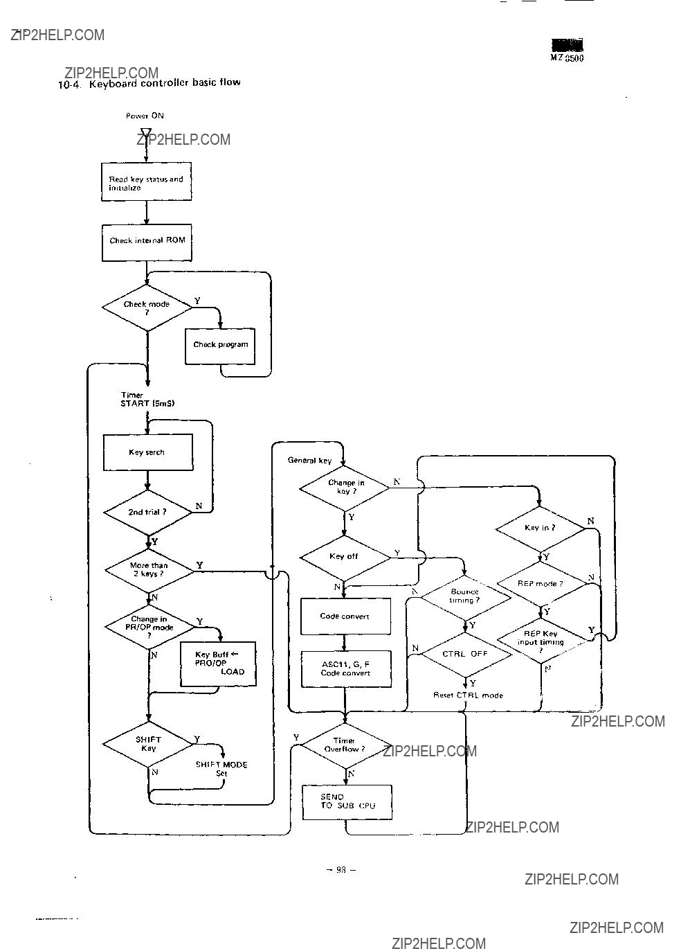
Power ON
Timer
START (5mS)
- 93 -

MZ3500
Function
Output data signal from the sub CPU (D(O)
Internal clock oscillator crystal input
Internal clock oscillator crystal input
Processor initialize
+ 5V
Strove of D(C) that also is used for interrupt to the keyboard side (ST(O)
GND
NC
NC
NC
NC
RETURN signal from the keyboard is input when a key is pushed during key search
0V supply
Output data signal from key (D(K))
Strobe of D(K) which also is used for interrupt to the CPU side (ST(K))
Not used
NC
+ 5V
Strobe to the keyboard unit by which a hexadecimal code is sent out for generation shift pulses to terminals X O X 1 5 o f t h e 4 5 1 5 decorder during key search
NC
Pins used to activate the keytop embeded LED #32 pin Alphabets and symbols (LOCK) #33 and #34 are not used
Not used
Keyboard type identifier pin Keyboard type is identified by mears of KSO, KS1, KS2 of KUC1 an KUS2. whether it is GND or NC
Acknowledge input from the CPU (ACK(O) Sent only when the CPU receives a correct data
+ 5V supply
11. SELF CHECK FUNCTIONS
The
Test regarding the main CPU
1)MFD I/F. 128KB RAM. 16KB ROM (for ROM based machine) checks
[Procedure]
LED (fof id??niific??Tion of GO/NO GO)
1.Turn on all dip switches of the 4 bit switch (located in the middle of the front side of the board) and turn on all dip switches of the 2 bit unit on the front side of the board.
2.Insert a floppy disk into drive unit No 2 (the third drive unit)
3.Turn the power on
4.The LED flickers for a moment then the test program starts During execution of the test program, the LED stays unlit About four seconds later the result is
mdicsted (DISPLAY)
(1)LED comes activated after normal ending of the test
(2)LED flickers after abnormal ending of the test
The kind of error can be known by how the LED is activat ed and flickered

Type of error
0)MDF 1/F error
ON OFF
1sec. 4sec.
(2.1 SDO read/write error
(3)SDO bank alternation error
??AD2 bank alternation error
?? AD3 bank alternation error
CD ROM
??Option RAM read/write error
(Indicated even when the option RAM is not in use)
/s~. Option RAM bank alternation error
NOTES:
1.The MFD I/F will not be tested, if there is no MFD I/F connected or when the diskette was not inserted in the slot of the drive unit No.2.
2.ROM test will not be performed, unless it is a ROM
based machine.
2) Loacing check program
The test program is loaded from the specified track and
sector to start executing the test.
[Procedure]
(1)Set dip switches on of the 4 bit unit located in middle of the front side of the board as illustrated at the right.
POSITIONOFF ON ON ON
,2) Set dip switches on of the 2 bit unit located on the
front side of the board.
(3)Insert the media into a slot of any diskette drive unit.
(4)Turn the power on
(5)Load the program from the specified track and sector,
to start execution of the test program.
[Conditions required for the drive unit and media]
(1)Use the
(2)Program may exist in any sector of any track, provided that it is written in continuous sector within a same track.
(Max. 256 bytes x 16 sectors = 4K bytes)
(3)Data descrived next should have been written on Sector 1 of Track 0.
(4)Program loading address must be 4800H and higher

MZ 3500
Sector 1, Track 0 information
Single dencity (Track 0)
No of data transfers = INT [IOCS capacity/1 K] + 1
Double density (other than Track 0)
???
SIDEless than eight blocks, the block following to the final
SIDE 1 (reverse side)
block mut be traced by "FFH".
[Test items]
Memory, VRAM, GDC peripheral, clock, speaker, printer interface, light pen. and RS232C interface.
GO/NO GO of the test must be confirmed on the video screen. Moving from test to test is done by depressing the HALT key.
POSITION OFF ON ON
[Procedure]
(1)Turn OFF all dip switch of the 4 bits unit located in the middle of the front side of the board and turnOFF all dip switches of the 2 bits unit.
(2)Set the system dip switch levers (10 bits) located on the reverse side of the board to the foilowing positions.
ON ON OFF OFF ON ON ON
(3)Turn power on while pushing the HALT siwtch to start the test program. Then, push the HALT switch to step to each test phase.
Result of GO/NO GO will appears on the video screen, except for the CRT interface and speaker tests.

1) Memory test
[Display]
(1)Normal test ending
RA OK:
RA OK
Shared RAM
RA OK
Above information are displayed on three display lines.
(2)Abnormal test ending
RA ER
3)CRT inter face test
Performance of the CRT is tested. To move into each test phase, push the HALT switch. Test
CRT.
'Procedure and display] (TestNo.1)
Confirm all patterns on the display screen of 40 digits and 20 lines.
(Test No.2)
Confirm all patterns on the display screen of 80 digits and 25 lines.
(Test No.3)
(1)Confirm that an entire screen is Filled with "H".
(2)Confirm that attributes areshown asillustrated.
2)VRAM check
Proceed to test for ASCI! and atnbute VRAM [Display]
During test penode, display shows under following.
(1)Display reviced "U" for entire screen Irom top side.
(2)Display blinking "I'' with under! ne for entire screen.
(3)Display entire screen by space.
Test end
1.Normal
VR OK
2.Abnormal
VR ER
8
9
0
Vertical line
Horizontal line
Highlight
Blink
- 97 -
MZ3500
( Check No. 4 )
Border in black
!??? "H" in whi
Backroung in red
L "H" in blue
L "H" in green
[??? "H" in white
4) Speaker test
Performance of the speaker and the volume control are tested. Listen carefully to detect any abnormal sound or mulfunction. Adjust the volume control to a suitable listen- ing level.
5) Printer interface test
Performance of the printer interface signal lines and action of the 8255 are tested.
[Dispaly]
(1)Normal test ending
PR OK
(2)Abnormal test ending
PR ER
6)Light pen interface test
Performance of light pen interface signal lines and the action of the GDC are tested.
[Display]
On the upper left corner of the screen is displayed character and line.
(1)Normal test ending
LP OK
(2)Abnormal test ending
LP ER
7)RS232C interfacetest
Performance of RS232C interface signal lines and the action of the 8251 are tested.
[Display]
(1)Normal test ending
RS OK
(2)Abnormal test ending
RS ER
( Check No. 5 )
Kff
"H" inred
"H" in green
"H" in white
^n O_ 1 _ 5 c *^ O" 2
RCD
SDR O.7 29
3
It will need wiring connection as illustrated in the figure in order to test the RS232C interface. Pins of the RS232C interface edge connector must be wired in the following manner:
Front side
/*
7 5 3 1
- 98 -

MZ3500
8)
MAIN CPU CHECKER FLOW CHART 1/2
( MAIN CUP A
CHECKERSTAHT ]
c
Write "66" ??nd~Of~ on Tracki 0.20.??^3
NOTE lnclud?? SEEK etroi and RECALIBRANTE
NOTE tr??c1i>d?? SEEK error and RECALIBRATE
- 99-

MZ3500
MAIN CPU CHECKER FLOW CHART M?
Option HAM
read/write check
Change bank of the option RAM
Error
on display
C HALT
- 100 -

M7*500
SUB CPU CHECKER FLOW CHART 1/3
( SUB CPU ^
CHECKER START I
CRTmt*f face t??t
SeiGDCto??00<amr.
- 101 -

MZ3500
SUB CPU CHECKER FLOW CHART 2/3
Sei th?? timer to 23 hourt. 59 minuiei. 58 **corxii
Oc*mb??r 3 III
Printer int M??c* tt??t
SUB CPU CHECKER FLOW CHART 3/3
1)Keyboard controller ROM test
(1)After power on in a normal condition, it starts to carry out the
If the alpha/symbol (LOCK) LED were to turn on, it indicates a failure in KBC. If not, KBC is satisfactory. t Key self check functional specification (simplified check)
2)Keyboard test
(1)As the power is turned on with the "DEB" in depres- sion, it goes into the keyboard
(2)Depress key in a given sequence. If key is depressed in a correct sequence, it makes the alpha/symbol (LOCK) LED activated each time a key is pushed.
If the key was pushed in a wrong sequence or when a failure is met in the key, it makes the LED blinked.-
(3)It returns to the normal mode upon completion of testing all keys. With this, the LED goes out.
(4)Observe the following
i)Turn the OP/PRO siwtch to the OPside.
ii)Turn on power while pushing the "DEB" key.
iii)Turn the PO/PRO which to the PROside.
iv)Push a key one at a time in accordance with the given sequence.
- 102 -
MZ3500
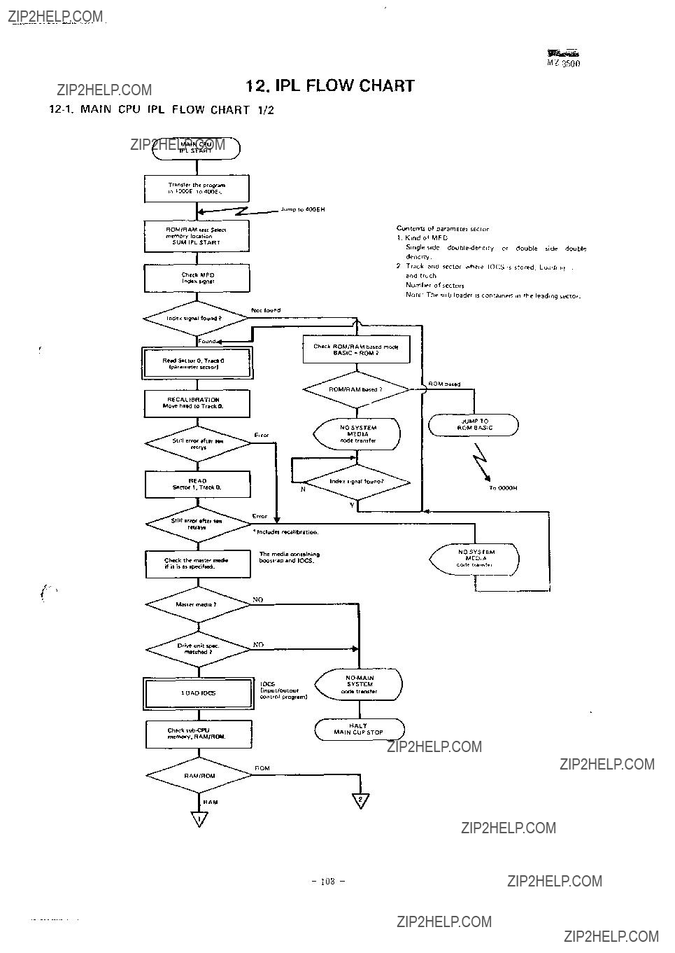
12. IPL FLOW CHART
( MAIN CPU ^
(PL START J
Transfer the program m
B Jump to 400EH
ROM/RAM test S**ect memory location
SUM IPL START
Check MFD
Index itgnal
Contents of parameter sector
1.Kind of MFD
2.Track and sector where IOCS is stored, Loadi vj '. and Truch
Number of sectors
Note' The sub loader is contained m the leading sector.
- 103 -
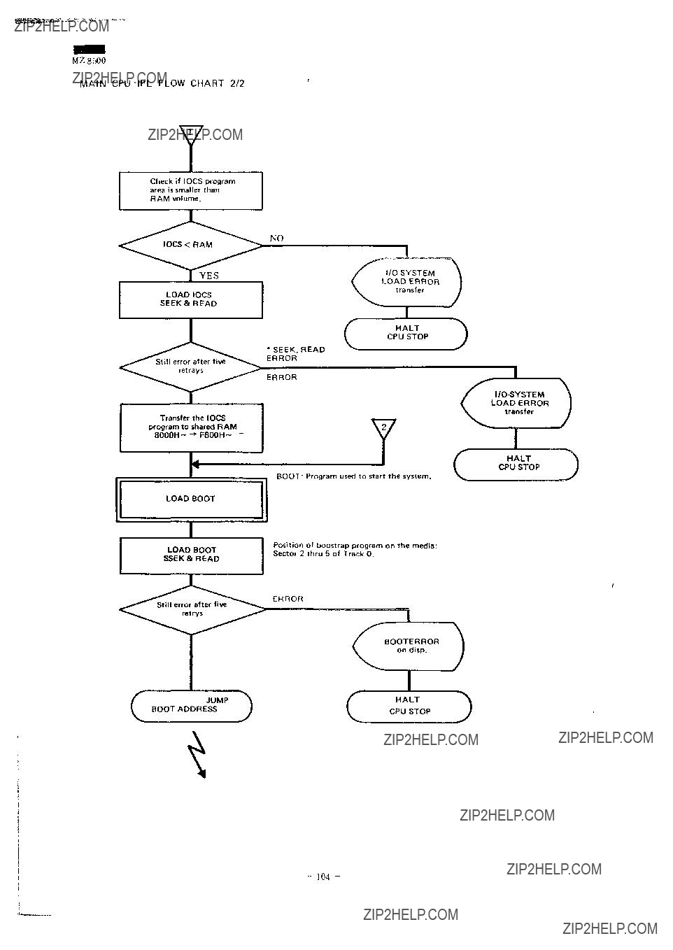
MZ3500
MAIN CPU IPL FLOW CHART 2/2
I
Check if IOCS program area is smaller than RAM volume.
NO
YES
LOAD IOCS
SEEK& READ
Transfer the IOCS program to shared RAM
LOAD BOOT
LOAD BOOT
SSEK& READ
ret rys ^ ???
JUMP ^\
BOOT ADDRESS )
I/O SYSTEM
LOAD ERROR transfer
c HALT
CPU STOP
???SEEK, READ
ERROR
ERROR
BOOT: Program used to start the system.
Position of boostrap program on the media: Sector 2 thru 5 of Track 0.
ERROR
1
CBOOTERROR on disp.
*
- 104 -

122. SUB CPU IPL FLOW CHART
( POWER ON A
SUB CPU IPL J
T,m??,
1
In t,alize8255
A Mode 0.8 Mode 1.
C OUT
1
SUB CPU READY OFF
1
Rest GDC
1
Check ROM sum
Initialize GDC and check G VRAM
Set the custom LSI CSPI and
CSP2 control boards
Initialize GDCagatr
IPL ROM is broke u indicated on display
- 105 -

74 LS 00
m R R R R R F1
LJ LJ U U U LJ U
IA IB \\ A H ^> ( M
m m
LJ LiJ LiJ LJ LL! LiJ LJ
1 Y IA IB 2Y 2A 2B C^D
74 LS 03
Vet +B 4A 4Y 3B 3A 3Y
LJ LJ LJ LJ LJ LJ LJ
IA IB 1Y 2A 2B 2Y GND
74 tS 04
6A 6Y SA^ 5Y 4A 4Y^
LJ LJ LJ LJ LJLJ LJ
IA IY 2A 2Y 1A 1Y CM>
74 IS 08
\tc 4B 4A 4Y 3B 3A IY
LJ LJTJLJ LJ LJ LJ
IA IB I Y 2A 2B 2Y GN1>
Vg 1C IY 3C 3B 3A 3Y
M R R R R R m
jTj UTJ LJ LJ LJ
IA IB 2A JB ^C 2Y CM>
PARAI IH if
sim i/ INIVT airuT ^~
Va I OAJ H UH (,
1C 1AI 2Y4 IA?? 'V3 IA3 'Y' IA4 2Y] CM
NtC K 1Y1
JjuJTUL??J I sITTTT' I I ej LH T??I
1C IA1 2Y4 1A2 2Y3 1A3 2Y2 lAi ZY] GND
LULU LD LJ LU LU LU LJ LU Lll
LJLJLJLiJLJLJLJLJLJL J
CLEAW 1Q ID 2V 2Q 3Q 3D 4Lt *Q GND
16

M 7. - 3500
171m nyi ryirTi n
UUU LJ U U LT
U U U LJ U U U
I 'K IK l>
/^PDI 99OC
\l
m M M r^n R m
LU L^JHI L??J 111LlJ LJ
<. 2 l~l LO S 1 )t (_S |)| N IAD
T A 7 3 1 3
19
UPHc
17D \\7
16D \\8
D ws- 1 >
1.D \ < \M'C
D M} 'u i C f. 103 V. \\2C 7
K \M
14 D' "i
13D 1 <>2
12 3 1 03
H D 1 <>4
D??h10
64K 0 3 B
65HDD
66(.1 k
67K 0 4 B
68M P X
69(,M>
70C ASB
20

PARTS GUIDE LI
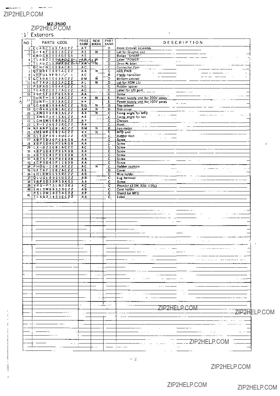
li Exteriors
NO PARTS CODE
1C C A B C 1 0 0 7 A C Z Z
2G F T A F 1 0 0 1 A C Z Z
31 H B D G B 3 0 0 4 G E S A
4| T L A B Z 1 0 0 3 A C Z Z
!> T L A B Z 1 0 0 8 A C Z Z
6Q C N C W 1 0 0 8 A C 0 1
7Q P W B F 1 0 0 5 A C Z Z
8V H P G L 9 P R 2//- 1
9G C A B A 1 0 0 3 A C Z Z
10G F T A U 1 0 0 5 A C Z Z
11P S P A G 1 0 0 4 A C Z Z
12T L A B Z 1 0 1 7 A C Z Z
16X B P S F 3 0 P 0 6 K O O O U N T - 1 0 1 8 A C Z Z
D U N T - 1 0 3 5 A C Z Z
18G C A B B 1 0 0 4 A C Z Z
19G C O V H 1 0 0 1 A C Z Z
20L A N G T 1 0 0 3 A C Z Z
21L A N G T 1 0 1 0 A C Z Z
22L C H S M 1 0 0 8 A C Z Z
23L X - l Z 6 0 2 3 R C Z Z
24N F A N P 1 0 0 1 A C Z Z
25R M E M R 1 0 0 2 A C Z Z
26G L E G P 0 0 1 0 U C Z Z
27X B P S D 3 0 P 0 8 K S O
28X B P S D 4 0 P 0 6 K S O
29L
30X B P S D 4 0 P 0 6 K O O
31X B T S C 4 0 P 0 6 0 0 0
32X B T S F 4 0 P 0 8 0 0 0
33X C P S D 4 0 P 1 2 0 0 0
34P H O G - 1 0 0 1 A C Z Z
35G F T A F 1 0 0 2 A C Z Z
36L H L D W 6 6 5 5 R C Z Z
37Q L U G L 0 0 0 6 U C Z Z
38X B P S D 3 0 P 3 0 K S O
39VR
40L H L D W 6 6 5 5 R C Z Z P S L D M 1 0 0 3 A C Z Z T L A B Z 1 4 0 0 C C Z Z
D E S C R I P T I O N
series series
1
1
I

oe

[2] PWB & Fixing angles
8X B P S D 3 0 P 0 6 K O O A A D U N T K 1 0 8 2 A C Z Z
**
9D U N T K 0 8 3 A C Z Z
**
NC Fixing angle for speaker C Connector
NB HALT switch
B Variable resistor C Speaker
C Screw
E CPU PWB unit (Model 3541)
NC Connector for CRT
C Screw
NC Insulator for MFD C Connector
NC Connector (18pm) C Screw
C Screw
32


,5! CPU PWB
[6] Power supply unit


