GSM TELEPHONE
GSM TELEPHONE

Contents
1. Safety Precautions
2.General Introduction
3.Specification
5.Circuit Description
6.TEST Command & Test Procedure
Contents
9.MAIM Electrical parts list
10.Flow Chart of Troubleshooting and Circuit Diagrams
11.PCB Diagrams
12.Block Diagrams
13. Reference data

This Service Manual is a property of Samsung Electronics Co.,Ltd. Any unauthorized use of Manual can be punished under applicable International and/or domestic law.
??? Samsung Electronics Co.,Ltd.
Code No.:
2006. 08. Rev.1.0

1. Safety Precautions
???Repair in Shield Box, during detailed tuning. Take specially care of tuning or test,
because specipicty of cellular phone is sensitive for surrounding interference(RF noise).
???Be careful to use a kind of magnetic object or tool,
because performance of parts is damaged by the influence of manetic force.
???Surely use a standard screwdriver when you disassemble this product, otherwise screw will be worn away.
???Use a thicken twisted wire when you measure level.
A thicken twisted wire has low resistance, therefore error of measurement is few.
???Repair after separate Test Pack and Set because for short danger (for example an overcurrent and furious flames of parts etc) when you repair board in condition of connecting Test Pack and tuning on.
???Take specially care of soldering, because Land of PCB is small and weak in heat.
???Surely tune on/off while using AC power plug, because a repair of battery charger is dangerous when tuning ON/OFF PBA and Connector after disassembing charger.
???Don't use as you pleases after change other material than replacement registered on SEC System.
Otherwise engineer in charge isn't charged with problem that you don't keep this rules.
SAMSUNG
This Document can not be used without Samsung's authorization
Safety Precautions
Several semiconductor may be damaged easilly by static electricity. Such parts are called by ESD(Electrostatically Sensitive Devices), for example IC,BGA chip etc. Read Precaution below. You can prevent from ESD damage by static electricity.
???Remove static electricity remained your body before you touch semiconductor or parts with semiconductor. There are ways that you touch an earthed place or wear static electricity prevention string on wrist.
???Use earthed soldering steel when you connect or disconnect ESD.
???Use soldering removing tool to break static electricity. otherwise ESD will be damaged by static electricity.
???Don't unpack until you set up ESD on product. Because most of ESD are packed by box and aluminum plate to have conductive power,they are prevented from static electricity.
???You must maintain electric contact between ESD and place due to be set up until ESD is connected completely to the proper place or a circuit board.
SAMSUNG
This Document can not be used without Samsung's authorization

2. General Introduction
The
<Specification>
<GPRS/EGPRS Factor>
???MS Class
???GPRS Phase
???
???SMG
:Class B
:GSM Phase II+
???Coding scheme : CS1 - CS4(GPRS), MCS5 - MCS9(EGPRS) support
???WAP 2.0 Browser
???SIM AT(Application Toolkit)
???40 Polyphonic Ringtone
<Basic Package >
???Handset + Standard Battery + TA + User Guide + Handstrap
<Option Item >
???Travel Adapter
???Ear Microphone
???Bluetooth Headset
???Bluetooth Hands Free Kit
???Car Charger/Adapter
SAMSUNG
This Document can not be used without Samsung's authorization

3. Specification
SAMSUNG
This Document can not be used without Samsung's authorization

Specification
SAMSUNG
This Document can not be used without Samsung's authorization

Specification
SAMSUNG
This Document can not be used without Samsung's authorization
4. Product Function
Main Function
alarms, calendar, task list, calculator, world time, unit conversion, timer, and stopwatch.
SAMSUNG
This Document can not be used without Samsung's authorization

5.Circuit Description
<RF Circuit Description of
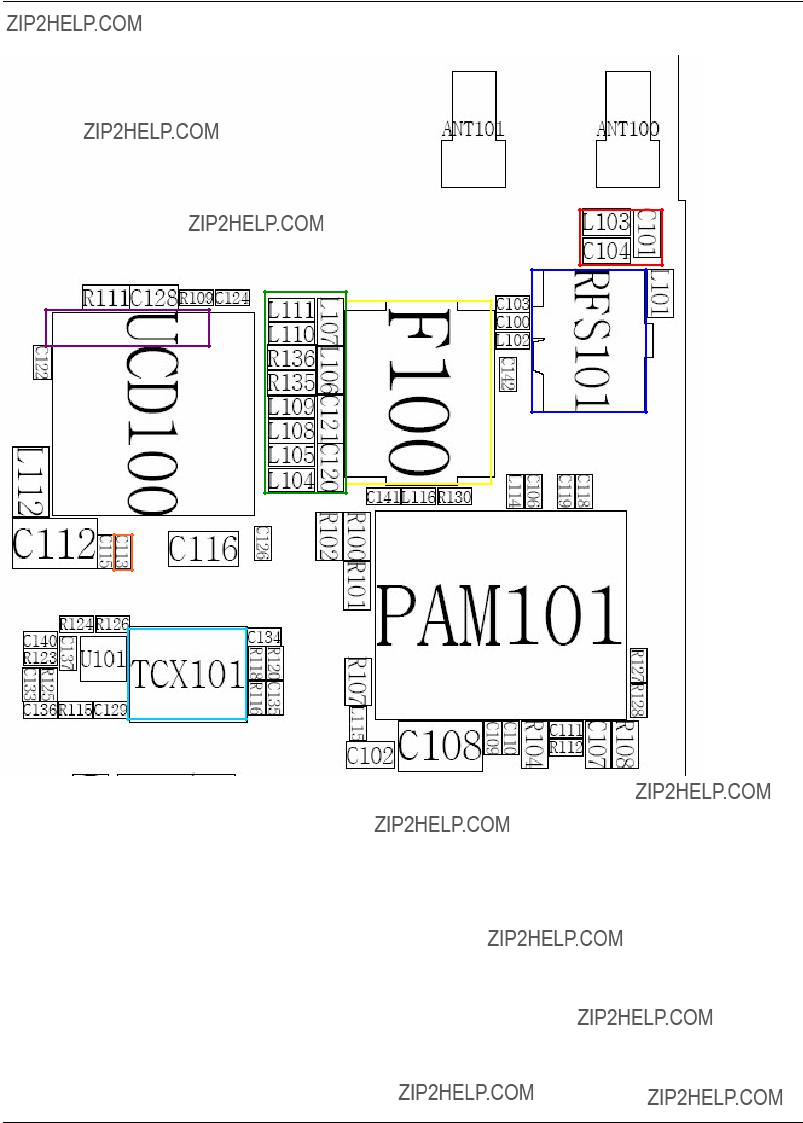
1.FEM (F100)
==> Switching Tx, Rx path for GSM850, EGSM900, DCS1800 and PCS1900 controlled by logic.
Integration of GSM850, EGSM900, DCS1800 and PCS1900 RX SAW Filters.
To convert Electromagnetic Field Wave to Acoustic Wave and the pass the specific frequency band.
-for filtering the frequency band 824 ~ 849 / 869 ~ 894 MHz
-for filtering the frequency band 880 ~ 915 / 925 ~ 960 MHz
-for filtering the frequency band 1710 ~ 1785 / 1805 ~ 1880 MHz
-for filtering the frequency band 1850 ~ 1910 / 1930 ~ 1990 MHz
2.FEM Control Logic
==> Truth Table
3.
==> To generate the 26 MHz reference clock to drive the logic and RF.
4.SKY74137 (UCD100)
==> The sky74137 is a RF tranceiver IC for GS850, EGSM900 DCS1800
and PCS1900 quardband cellular systems, and incorporates EDGE tranceiver capabillity, and integrates most of the low power silicon functions of a tranceiver. The receive path implements a direct downconversion architecture. The transceiver consists of four integrated Low Noise Amplifiers (LNAs), a quadrature demodulator, selectable baseband filter bandwidths, and lowdroop DC Offset Correction (DCOC) sequencer.
- RX Function
Four LNAs which support different bands of operation have separated differential inputs. The LNA outputs feed into a quadrature demodulator that
SAMSUNG
This Document can not be used without Samsung's authorization

Circuit Description
- TX Function
The device implements Skyworks Polar Loop transmit architecture. This architecture autonomously splits the amplitude and phase within the device using the traditional analog
5. POWER AMP (PAM400)
The module consists of a EGSM850/900 PA block and a DCS1800/PCS1900 PA block, Both PA blocks share common power supply pins to distribute current. The subsystem consists of two parts : a Power Amplifier Control (PAC) block, and an Integrated Coupler. To select GSM900/850 and GMS1800/1900 as determined from the Band Select (BAND_SEL) signal. SKY77331 contains band select switching circuitry to select GSM (BAND_SEL is low) and DCS/PCS (BAND_SEL is HIGH) as determined from the Band Select (BAND_SEL) signal. The BAND_SEL pad selects the PA output (DPCS_OUT or GSM_OUT) while the Power Control (VPC) controls the level of output power. The integrated power amplifier control (PAC) function provides envelope amplitude control by reducing sensitivity to input drive, temperature, power supply, and process variation.
< Baseband Circuit description of
1. CSP2750 (UCD301)
==> The CSP2750 has two major logical components power management and conversion signal processing.
The PSC component is responsible for all
???Power management for RF, BB and ancillary devices within the GSM/GPRS
???
???Reset control
???SIM card
The CSP component is responsible for the following ;
???Intraframe event scheduling
???Voice band processing, including voice band ADC and DAC
???Analog baseband processing, including baseband ADC and DAC
???Providing RF interface for Trident digital baseband device
???Transmitter Power control
???Automatic frequency control
???A5 ciphering
???
The CSP2750 has the following major physical components;
SAMSUNG
This Document can not be used without Samsung's authorization

Circuit Description
???Timing and control unit
???RF serial interface
???
???Baseband Transmitter / Receiver
???Voice input and output
2.WM8955L(UCD401)
==> The WM8955L is a low power, high quality stereo DAC with intergrated headphone and loudspwaker amplifiers, designed to reduce external component requirements in portable digital audio application.
The
The WM8955L can operate as a master or a slave, and include an
The WM8955L operates on supply voltages from 1.8V up to 3.6V, although the digital core can operates on a separate supply down to 1.42V, saving power. Different section of the chip can also be powered down under software control.
3. HPE(UCP201)
==> The
The
??? 101 MHz system bus, 16 kbyte instruction and 16kbyte data caches.
??? 8 kbyte tightly coupled zero
??? direct memory access controller for transparent transfer between memory and peripherals.
??? External Memory interface with asynchronous burst mode support
SAMSUNG
This Document can not be used without Samsung's authorization

Circuit Description
???Synchronous serial port supporting
???Programmable
???SD/MMC controller that supports interfacing to secure digital/multimedia memory card. Two DSP16000
???Memory complement;
-DSP0 : 144K X
-DSP1 : 96K X
JTAG boundary scan and integrated H/W developement system Low power;
???Ultralow leakage process technology for
???Flexible power management modes to allow for maximum active power management Interprocessor communication hardware support between ARM, DSP0 and DSP1.
Supported by
- one for ARM and DSP, the other one for USB.
SAMSUNG
This Document can not be used without Samsung's authorization

6. Test Command & Test Procedure
-HP 8960
-DC Power Supply
-Test Jig
-Configuration
DC POWER SUPPLY
GPIB
- Samsung internal software
SAMSUNG
This Document can not be used without Samsung's authorization
Test Command & Test Procedure
- GMSK
1)Procedure:
a.Calibraion equipment HP8960 and the cell phone are connected through RF cable.
b.Target power ( required power level according to the specification which should be set by calibration program) is set to equipment as power level (ex: GSM 5 level is 32.5 dBm).
c.Activate phone in Tx_Mode_Only.
d.HP8960 equipment measures transmitted power through rf test cable from the phone and reports measured level to calibration program.
e.The program compares measured power with the target power.
f.The calibration program decides power code which is defined in advance in the program and writes the codes to the flash memory in the phone.
2)Target value is defined according to the value of GSM specification. See the TX power level definition table below.
3)Target values of the peak level of the phone are set normally in conducted mode
- GSM850 5 level : 32.5dBm
- EGSM900 5 level : 32.5dBm
- DCS 0 level : 29.5dBm
- PCS 0 level : 29.5dBm (Tolerance :
4)Accuracy
All the TX level from the phone after
5) TX ramp mask specification applied to the calibration program :
SAMSUNG
This Document can not be used without Samsung's authorization

Test Command & Test Procedure
- 8PSK
1) Procedure:
a. Calibraion equipment HP8960 and the cell phone are connected through RF cable.
b. Target power ( required power level according to the specification which should be set by calibration program) is set to equipment as power level (ex: GSM 8 level is 27 dBm).
c. Activate phone in Cont_8psk_Tx_Mode_Only.
d. HP8960 equipment measures transmitted power through rf test cable from the phone and reports measured level to calibration program.
e. The program compares measured power with the target power. f. The calibration program decides power code which is defined in
advance in the program and writes the codes to the flash memory in the phone.
2) Target value is defined according to the value of EGPRS specification.
SAMSUNG
This Document can not be used without Samsung's authorization

Test Command & Test Procedure
See the TX power level definition table below.
3)Target values of the peak level of the phone are set normally in conducted mode
-GSM850 8 level : 27dBm
-EGSM900 8 level : 27dBm
-DCS 2 level : 26dBm
-PCS 2 level : 26dBm (Tolerance :
4)Accuracy
All the TX level from the phone after
5) TX ramp mask specification applied to the calibration program :
SAMSUNG
This Document can not be used without Samsung's authorization

7. Array course control
Test Jig
Test Cable
RF Test Cable
SAMSUNG
This Document can not be used without Samsung's authorization
Array course control
Software Downloading
???Two binary files for downloading T519.
???T519XXYY.s3 : Main source code binary.
???Downloader Program(OptiFlash.exe)
???T519 Mobile Phone
???Data Cable
???Binary files
SAMSUNG
This Document can not be used without Samsung's authorization

Array course control
1. Load the binary download program by executing the ???OptiFlash.exe???
2.Select the ???Options???
Choose hardware platform for the downloader file setting.
Set the everything else as the default values which are shown below
SAMSUNG
This Document can not be used without Samsung's authorization

Array course control
3. Select the COM port when the download cable is connected
Up to 64 ports are supported. Additionally you can select the maximum transfer speed OptiFlash will use to communicate with the phone. However, OptiFlash will use a slower speed if either the PC???s or the phone???s serial hardware is incapable of handling the selected speed.
SAMSUNG
This Document can not be used without Samsung's authorization
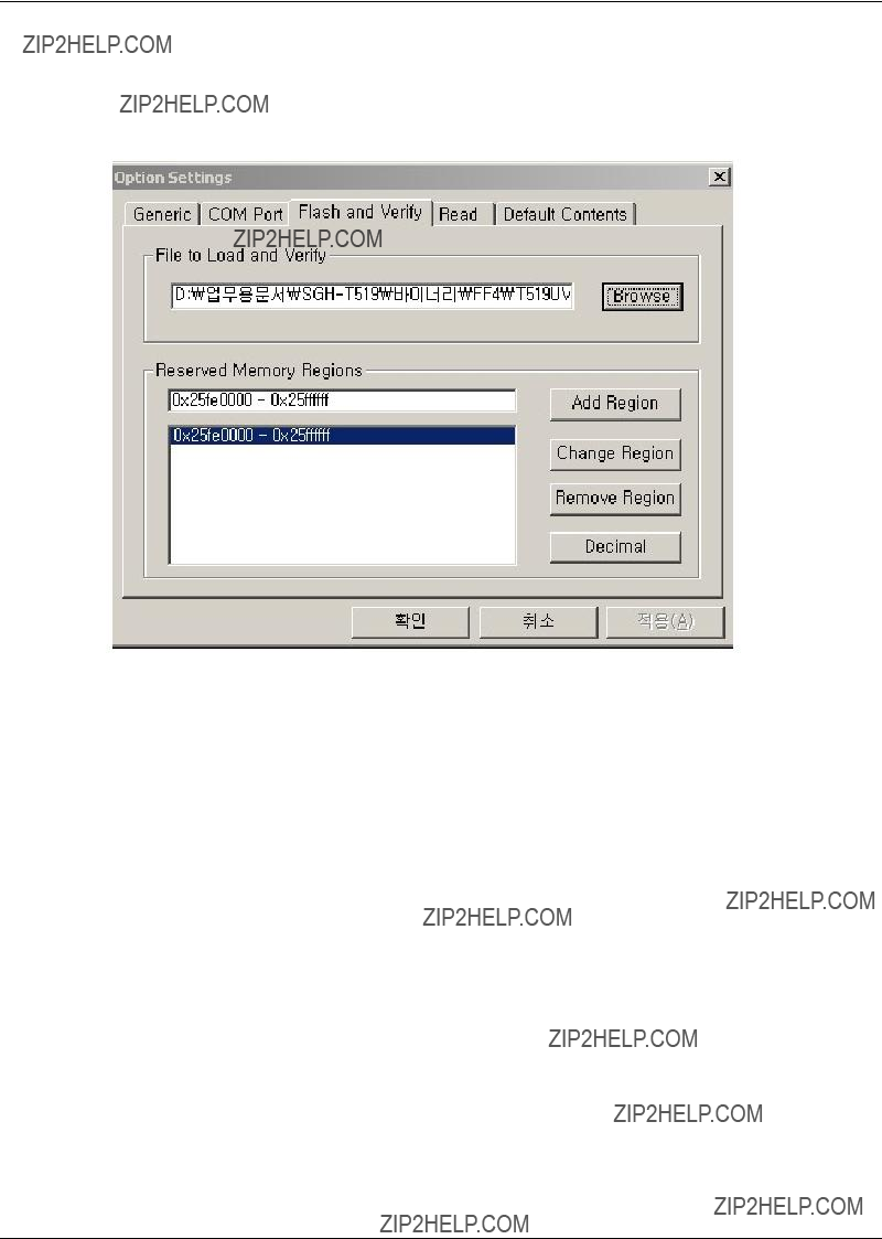
Array course control
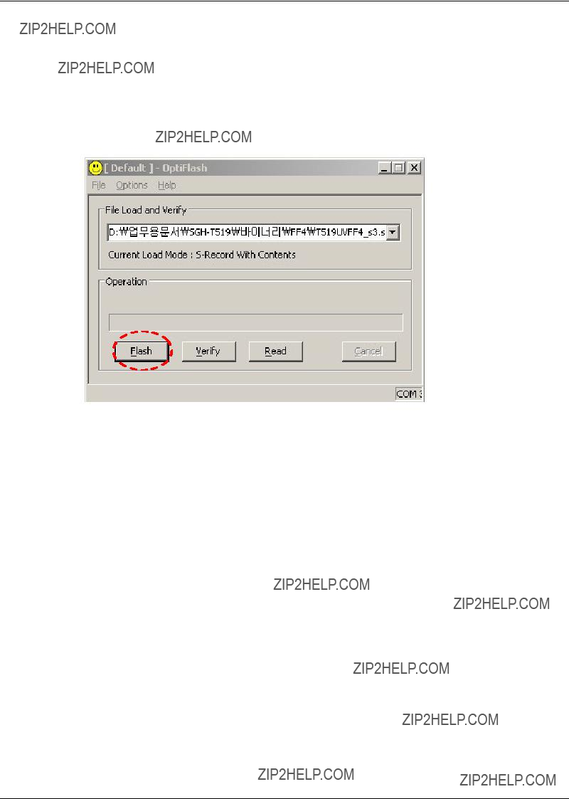
4.Select the???Flash&Verify???
Set the directory path and choose the latest s/w binary, for example ???T519XXYY.s3???, for the downloader binary setting.
In case of D407 the reserved regions are not a necessity. (It is defined in platform.def file)
SAMSUNG
This Document can not be used without Samsung's authorization
Array course control
5.Click ???OK??? button then press ???Flash???.
(Before pressing ???Flash??? button, push the button ???*???and ???END??? at the same time. Then press ???Flash???.)
Downloader will upload the binary file as below for the downloading.
6.When downloading is finished successfully, there is a ???All is well??? message.
7.After finishing downloading, Certain memory resets should be done to guarantee the normal performance.
8.Confirm the downloaded version name and etc. :
*#1234#
Full Reset :
*2767*3855#
SAMSUNG
This Document can not be used without Samsung's authorization

8. Exploded View and its Partslist
SAMSUNG
This Document can not be used without Samsung's authorization
Exploded view and its Part list
SAMSUNG
This Document can not be used without Samsung's authorization
Exploded view and its Part list
SAMSUNG
This Document can not be used without Samsung's authorization

Disassembly and Assembly instructions
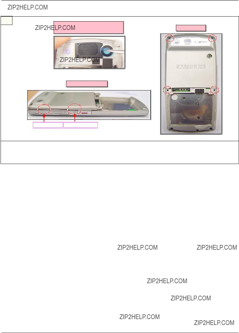
1.Remove a camera and SPK/MOT connector.
??? caution
1.Becarefulnottodamagetocameraconnectorpins
1.Detach a PBA Ass'y from LCD Module.
??? caution
1.Be careful not to do damage to intenna and scratch the LCD.
SAMSUNG
This Document can not be used without Samsung's authorization

Disassembly and Assembly instructions
7
1. Detach a LCD from LCD braket.
??? caution
1.Be careful not to do damage and scratch the phone.
SAMSUNG
This Document can not be used without Samsung's authorization
Disassembly and Assembly instructions
A.Remove a adhesive tape of EL sheet.
B.Attach a EL sheet
C.Attach a mic cover
D.Attach a key pad
E.Press a key pad
- Pressure kgf : 6 ?? 1 kgf/cm2
A.Examine the surface of rear,and attach a rear deco. and camera window.
B.Press a camera window.
-Pressure kgf : 6 ?? 1 kgf/cm2
3
1. Attach a SPK_MOT FPCB 
 2. Place a SPK_MOT FPCB
Connection part of SPK and MOT
Remove a adhesive tape
Base line when
attaching SPK
Place part printed ???,???into a groove
A.Connect SPK and MOT with FPCB and paste another FPBC along the baseline.
B.Place SPK_MOT
SAMSUNG
This Document can not be used without Samsung's authorization

Disassembly and Assembly instructions
4
soldering part.
A.Place a LCD inserting LCD connector on the front of CARRIER LOWER. B.Place a LCD into place hole of CARRIER LOWER correctly.
C.Press carefully the top (SAMSUNG logo) and bottom(
D.Attach a LCD sponge to CARRIER LOWER along the base line (the right side and bottom)
5
1. Soler side keys and stick a friction tape
A.Solder side keys with soldering jig.
B.Stick a friction tape along the baseline.
SAMSUNG
This Document can not be used without Samsung's authorization

Disassembly and Assembly instructions
Press the connector horizontally to a
PBA
A.Press carefully the top of PBA with your right hand grasping CARRIER LOWER with your left hand.
B.Press both sides of PBA until it clicks into the CARRIER LOWER. (Grasp the edge of LCD during work)
C.Press the LCD connector to the CARRIER LOWER horizontally.
A.Press the intenna until it clicks into the PBA
B.Put the SPK CONNECTER horizontally
C.Place the soldering part of INTENNA to a groove
SAMSUNG
This Document can not be used without Samsung's authorization

Disassembly and Assembly instructions
8
A.Solder the intenna with soldering jig
B.Place the camera into a groove of CARRIER LOWER.
C.Press carefully after placing camera module.
9
1.Place the PBA side keys
A.Place the PBA on the FRONT.
B.Remove the camera protection film.
C.Place side keys into place.
SAMSUNG
This Document can not be used without Samsung's authorization
Disassembly and Assembly instructions
SAMSUNG
This Document can not be used without Samsung's authorization

9. MAIN Electrical Parts List
This Document can not be used without Samsung's authorization

Electrical Parts List
This Document can not be used without Samsung's authorization

Electrical Parts List
This Document can not be used without Samsung's authorization

Electrical Parts List
This Document can not be used without Samsung's authorization

Electrical Parts List
This Document can not be used without Samsung's authorization
Electrical Parts List
This Document can not be used without Samsung's authorization

Electrical Parts List
This Document can not be used without Samsung's authorization

Electrical Parts List
This Document can not be used without Samsung's authorization

Electrical Parts List
This Document can not be used without Samsung's authorization

Electrical Parts List
This Document can not be used without Samsung's authorization
Electrical Parts List
SAMSUNG
This Document can not be used without Samsung's authorization
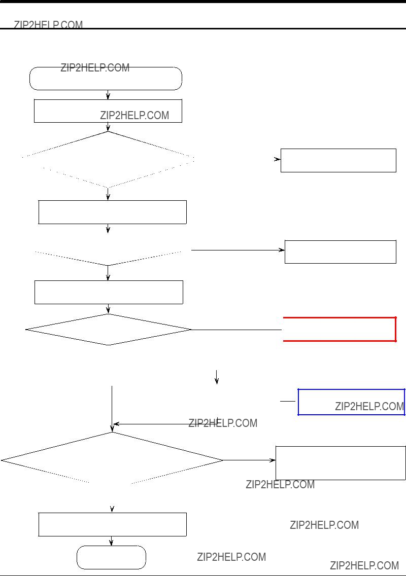
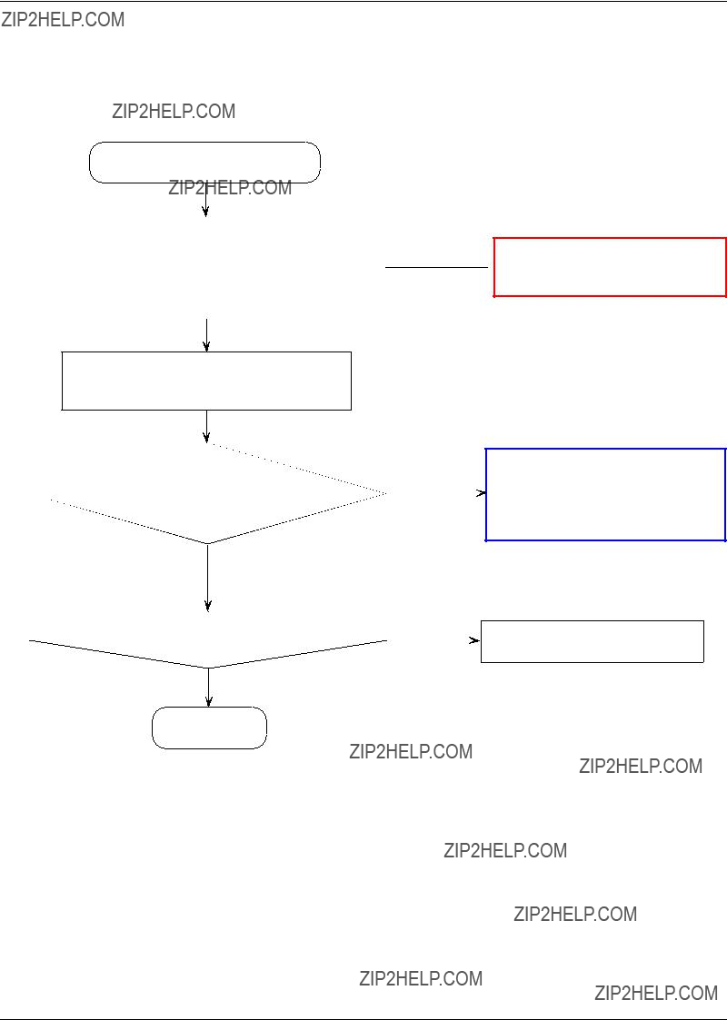
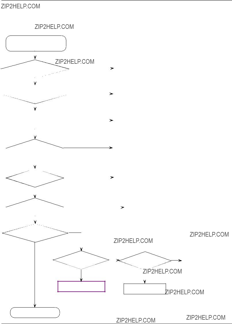
10. Flow Chart of Troubleshooting
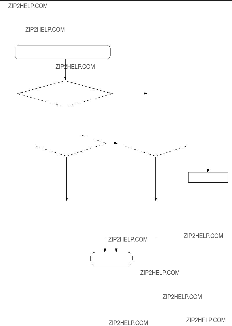
'Power ON' Does not work
Check the current consumption
YES
Check the V bat. voltage
Download again
Voltage ??? 3.3V ?
YES
NO
Charge the Battery
Check the pins of UCD301
???
C316 ??? 1.8V ?

 YES
YES
NO
 Check UCD301 and C316
C318 and C315 = 2.8V?
YES
NO
???
NO
C312=1.5V?
YES
 Check UCD301 and C312
Check the clock signal
at pin #3 of TCX101 or C129 Freq.=26MHz,Vrms ???300mV
 YES
YES
Check the Initial operation
END
NO
Check the clock generation circuit (TCX101, U101 pin#4)
SAMSUNG
This Document can not be used without Samsung's authorization

Flow Chart of Troubleshooting
DSP_DB(0:15)
EAR_CHECK
DSP_AB(0:8)
DSP_IO
DSP_RWN
FLASH_RESET
PCS_RX_EN
BAND_SEL
MOD_SEL
TX_EN
XOENA
SX_EN
PAC_EN
RX_EN
SERLE
SERDAT
SERCLK
UCD301
AFC
VAPC
RTX_IP
RTX_IN
RTX_QP
RTX_QN
CLK13M_MC
XOENAQ
CLK32K
SAMSUNG
This Document can not be used without Samsung's authorization
Flow Chart of Troubleshooting
SAMSUNG
This Document can not be used without Samsung's authorization
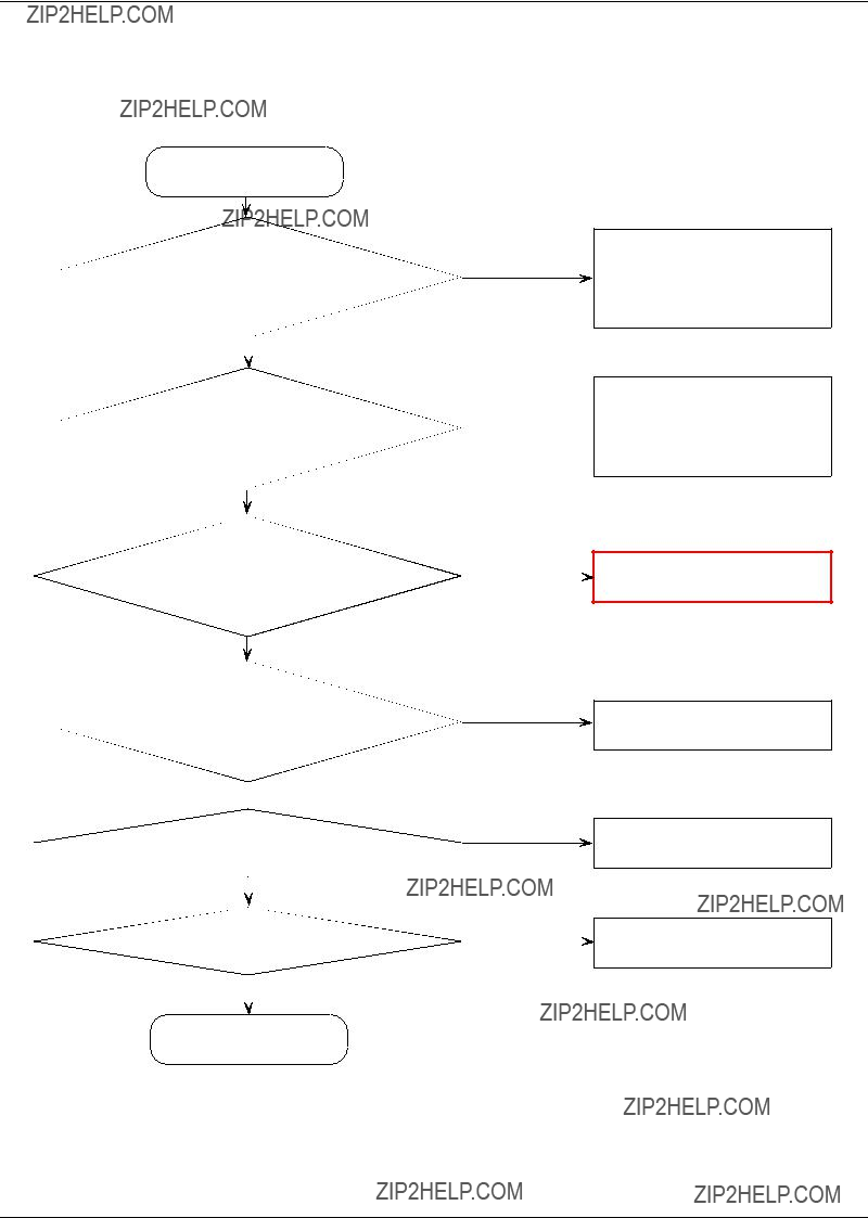
Flow Chart of Troubleshooting
Initial Failure
The voltage at the C316=1.8V?
NO
Check the UCD301
The voltage at the C315=2.8V?
 YES
YES
The voltage at the C216 " Low
YES
There is 32.768KHz wave form at the C222, C223 ?
YES
The voltage is 2.8V
at the C317,C313,C315,C318 ?
 YES
YES
LCD Display OK ?
 YES
YES
Sound operation OK ?
 YES
YES
END
(If it has some problem, it has to be replaced.)
Check the UCD301 NO  (If it has some problem,
it has to be replaced.)
???
NO
Check the UCP201
NO
Check the UCD301
NO
Check the LCD module
NO
Check the Audio part
SAMSUNG
This Document can not be used without Samsung's authorization
Flow Chart of Troubleshooting
A(0:25)
D(0:15)
CP_WEN
CP_OEN
SPCLK1_PIO18 M18
INT0 T15
CLK13M_TR
TR_RST
PCM_FSYNC
PCM_TXD
PCM_RXD
PCM_FCLK
DSP_INT
DSP_IO
DSP_RWN DSP_DB(15) 
DSP_DB(14)
DSP_DB(13) 
DSP_DB(12)
DSP_DB(11)
DSP_DB(10)
DSP_DB(9)
DSP_DB(8)
DSP_DB(7)
DSP_DB(6) 
DSP_DB(5)
DSP_DB(4) 
DSP_DB(3)
DSP_DB(2) 
DSP_DB(1)
DSP_DB(0)
DSP_AB(8)
DSP_AB(7)
DSP_AB(6)
DSP_AB(5)
DSP_AB(4)
DSP_AB(3)
DSP_AB(2)
DSP_AB(1)
DSP_AB(0)
VCCD_1.8V
CP_TDO
DSP_DB(0:15)
DSP_AB(0:8)
T_FLASH_ON
FLASH_RESET ROM1_CS ROM2_CS
RAM1_CS
MV3020_CS
LOWER_BYTE
UPPER_BYTE
CP_TMS
CARD_DETECT
BATTERY_OPEN_CHECK
MV3020_INT
JACK_INT
INTRQ
KEY_EL_EN
USB_CON
WM_SDIN
WM_SCLK
EAR_SWITCH
WM_CSB
ASW_SPEAKER
CHG_DET
DACPW_ON
LCD_BRIGHTNESS
XOENAQ
PWR_KEEP
CLK32K
RTCALARM
OSC201
1 2
MCI_DAT0_EN
MCI_DAT_EN
MCI_CMD_EN
MCI_DAT0
MCI_CMD
MCI_CLK
SAMSUNG
This Document can not be used without Samsung's authorization
Flow Chart of Troubleshooting
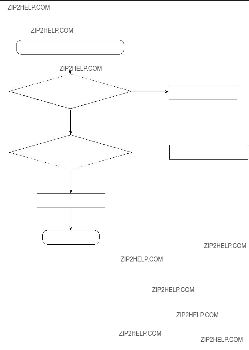
"Insert SIM" is displayed on the LCD
The voltage is 2.8V at C306?
YES
Is there any signal pin C305, C308, C309?
YES
Check the SIM Card
END
NO
Check the UCD301
NO

 Check the UCD301 & UCP201
SAMSUNG
This Document can not be used without Samsung's authorization
Flow Chart of Troubleshooting
ZD302
SAMSUNG
This Document can not be used without Samsung's authorization
Flow Chart of Troubleshooting
LCD display is abnormal
Check LCD connection and replace LCD
C338, C340 is 2.9V?
YES
pin#4 of ZD304 is LOW?
YES
Are there anysignal at pin#6 of ZD304?
YES
IS there any problem at F301, F302, F303, F304
NO
Check U400
NO
Check UCD301
???
NO
Check U400
NO
SAMSUNG
This Document can not be used without Samsung's authorization
Flow Chart of Troubleshooting
LCD_DATA(13)
LCD_DATA(14) LCD_DATA(15)
LCD_DATA(12)
LCD_DATA(11) LCD_DATA(10)
LCD_DATA(9) LCD_DATA(8)
LCD_DATA(7) LCD_DATA(6) LCD_DATA(5)
LCD_DATA(4)
LCD_DATA(3) LCD_DATA(2) LCD_DATA(1) LCD_DATA(0)
LED+_13.5V
MLCD_CS
LCD_ADS
LCD_WEN
SAMSUNG
This Document can not be used without Samsung's authorization

Flow Chart of Troubleshooting
LCD_DATA(5) LCD_DATA(6) LCD_DATA(7) LCD_DATA(8)
LCD_DATA(15) LCD_DATA(14) LCD_DATA(13) LCD_DATA(4)
LCD_D(5) LCD_D(6) LCD_D(7) LCD_D(8)
LCD_D(15) LCD_D(14) LCD_D(13) LCD_D(4)
LCD_DATA(9) LCD_DATA(10) LCD_DATA(11) LCD_DATA(12)
LCD_DATA(3) LCD_DATA(2) LCD_DATA(1) LCD_DATA(0)
LCD_D(9)
LCD_D(10)
LCD_D(11)
LCD_D(12)
LCD_D(3)
LCD_D(2)
LCD_D(1)
LCD_D(0)
SAMSUNG
This Document can not be used without Samsung's authorization
Flow Chart of Troubleshooting
Is the connection status of
HDC300 O.K?
YES
Check the DC bias voltage on
Mic path.
NO
???
 Reconnect connector of HDC300
???
The voltage of C406 is about 2.2V??10%?
YES
NO
Solder the microphone again or Replace
R406, R415, R418, R425
Is microphone OK?
YES
END
NO
Check UCD301
SAMSUNG
This Document can not be used without Samsung's authorization
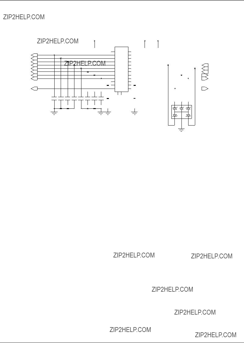
Flow Chart of Troubleshooting
EL_PWR
EL_PWR
KEY_COL(0)
KEY_COL(1)
KEY_COL(2)
KEY_COL(3)
KEY_COL(4)
MIC+
C310
DZ 013
PWR_ON
KEY_ROW(0)
KEY_ROW(1)
KEY_ROW(2)
KEY_ROW(3)
KEY_ROW(4)
MIC-
V 213
DZ 113
SAMSUNG
This Document can not be used without Samsung's authorization
Flow Chart of Troubleshooting
There is no sound from speaker
Is the connector
HDC401 O.K?
 YES
YES
Are there any signal at
L405, L406?
 NO
NO
Are there any signal at
R437, R438?
YES
YES 
???
NO
 Reconnect HDC401
Are there any signal
at the pin #15, 16 of UCD401?
NO NO
Replace UCD401
SAMSUNG
This Document can not be used without Samsung's authorization
Flow Chart of Troubleshooting
CLK13M_WM
C140
SAMSUNG
This Document can not be used without Samsung's authorization
Flow Chart of Troubleshooting
SAMSUNG
This Document can not be used without Samsung's authorization
Flow Chart of Troubleshooting
There is no sound from receiver.
Check UCD301
???
END
SAMSUNG
This Document can not be used without Samsung's authorization

Flow Chart of Troubleshooting
SAMSUNG
This Document can not be used without Samsung's authorization

Flow Chart of Troubleshooting
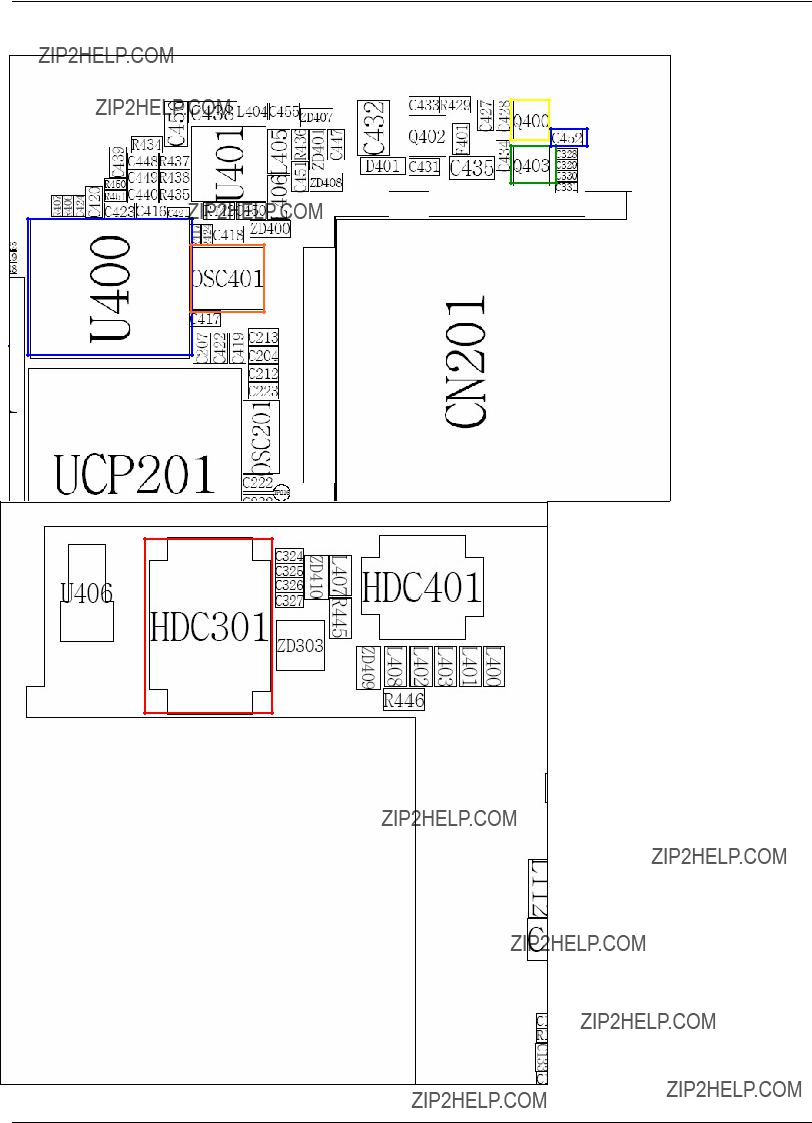
Camera function does not work
Is the connect HDC301 ok?
 YES
YES
C452 IS HIGH?
 YES
YES
Pin #3 of Q400 = 1.5V?
YES
Pin #3 of Q403 = 2.8V?
YES
???
Pin#3 of OSC401 is 24MHz?
YES
Is that clock signal at the pin #23 of HDC301?
YES
Pin#24 of HDC301 is High?
END
NO
SAMSUNG
This Document can not be used without Samsung's authorization
Flow Chart of Troubleshooting
CAM_D(0) CAM_D(1)
CAM_D(2) CAM_D(3) CAM_D(4) CAM_D(5)
CAM_D(6) CAM_D(7)
MCLK
C 423
C 723
C 823
VCAMIO_2.8VVCAM_1.5V VCAMA_2.8V
HDC301
ZD303
SAMSUNG
This Document can not be used without Samsung's authorization
Flow Chart of Troubleshooting
SAMSUNG
This Document can not be used without Samsung's authorization

Flow Chart of Troubleshooting
There is no MP3 sound from Earphone
Are there any signal at the pin #5,7 of IFC400?
NO
Are there any signal at R410, R411?
NO
Are there any signal
at the pin #10,13 of UCD401?
YES
???
 Check & Replace C457, C458
???
YES
???
Check UCP201
END
???
SAMSUNG
This Document can not be used without Samsung's authorization

Flow Chart of Troubleshooting
SAMSUNG
This Document can not be used without Samsung's authorization

Flow Chart of Troubleshooting
SAMSUNG
This Document can not be used without Samsung's authorization

Flow Chart of Troubleshooting
SAMSUNG
This Document can not be used without Samsung's authorization
Flow Chart of Troubleshooting
Continuous RX ON
RF Input : 62 CH
AMP :
???
UCD100 Change or resolder
UCD100 Check & resolder
Check UCD301
SAMSUNG
This Document can not be used without Samsung's authorization
Flow Chart of Troubleshooting
SAMSUNG
This Document can not be used without Samsung's authorization

Flow Chart of Troubleshooting
Continuous RX ON
RF Input : 62 CH
AMP :
???
UCD100 Change or resolder
UCD100 Check & resolder
Check UCD301
SAMSUNG
This Document can not be used without Samsung's authorization
Flow Chart of Troubleshooting
Continuous RX ON
RF Input : 62 CH
AMP :
???
UCD100 Change or resolder
UCD100 Check & resolder
Check UCD301
SAMSUNG
This Document can not be used without Samsung's authorization

Flow Chart of Troubleshooting
Continuous RX ON
RF Input : 62 CH
AMP :
???
UCD100 Change or resolder
UCD100 Check & resolder
Check UCD301
SAMSUNG
This Document can not be used without Samsung's authorization

Flow Chart of Troubleshooting
???YES
??? YES
YES
Change PAM101
SAMSUNG
This Document can not be used without Samsung's authorization

Flow Chart of Troubleshooting
SAMSUNG
This Document can not be used without Samsung's authorization

Flow Chart of Troubleshooting
???YES
??? YES
YES
Change PAM101
SAMSUNG
This Document can not be used without Samsung's authorization

Flow Chart of Troubleshooting
A TN 101
A TN 001
R SF 101
TA
BV
SGCD M 4747S 731 731 O_O_ TUTU
6
V CC
1 CN
4
CC
V
NO
CV
1
CF
A
31 B_M FU
C1 53
3
TU
O
DN
G
2
C 431
SAMSUNG
This Document can not be used without Samsung's authorization
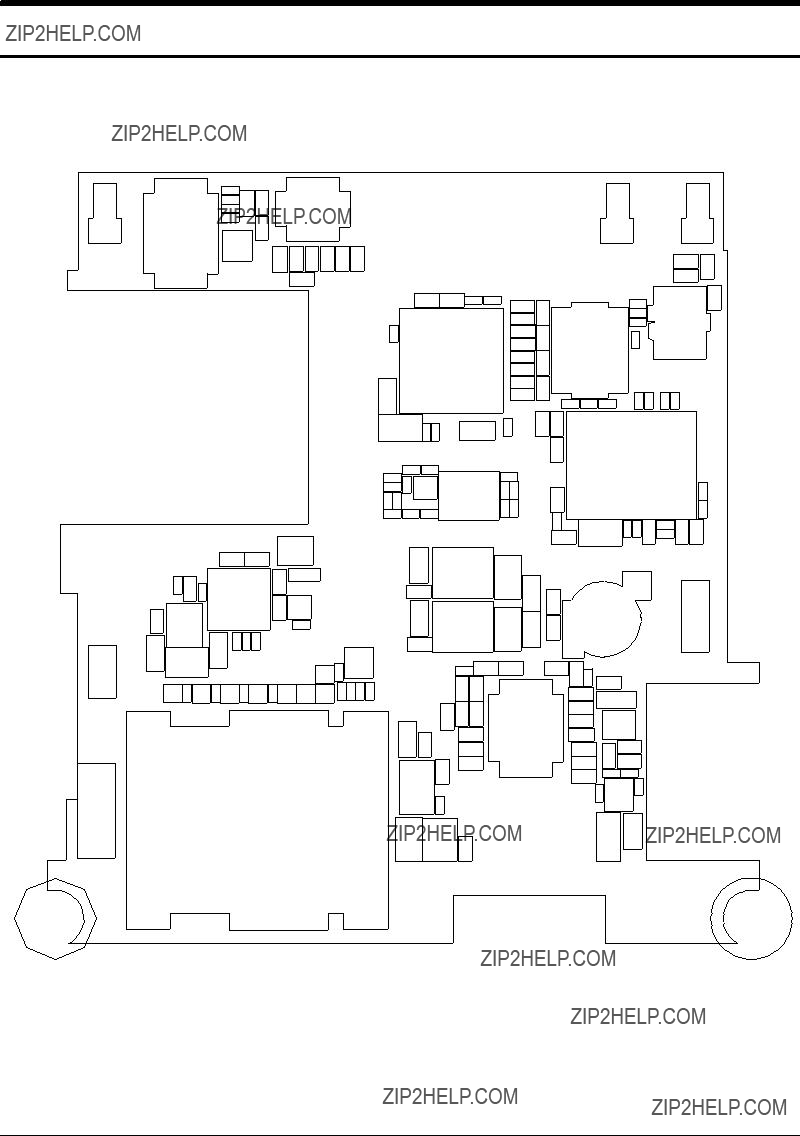
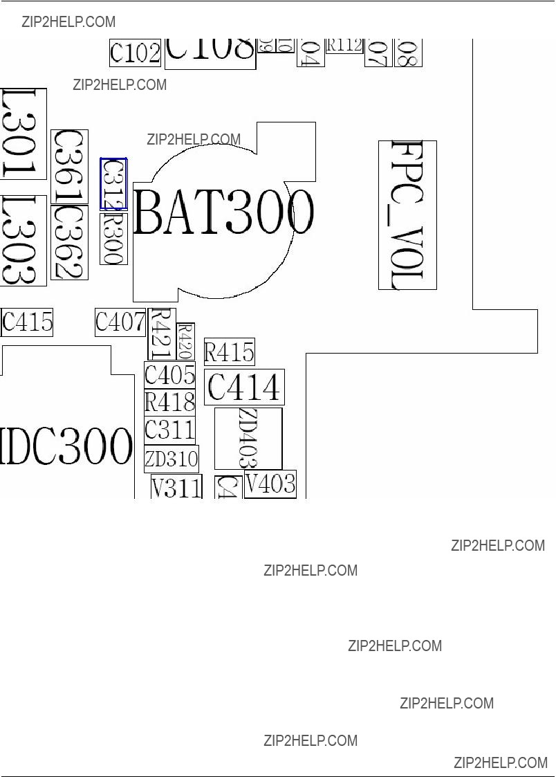
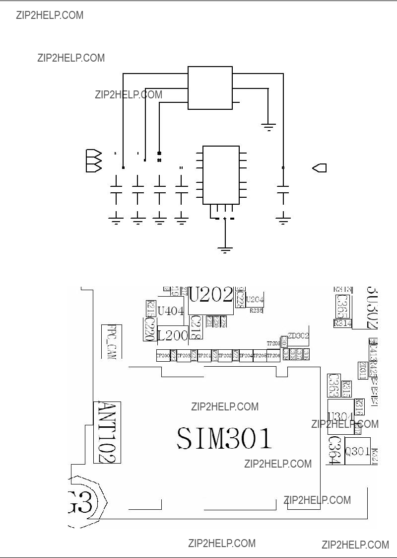
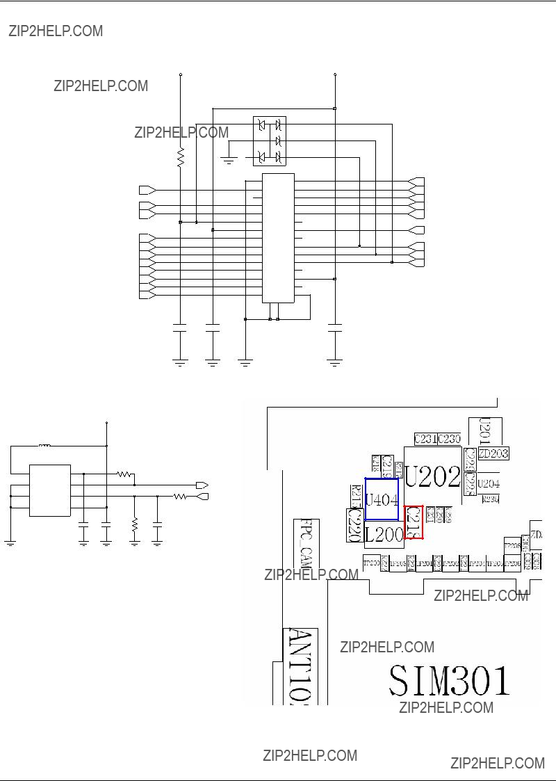
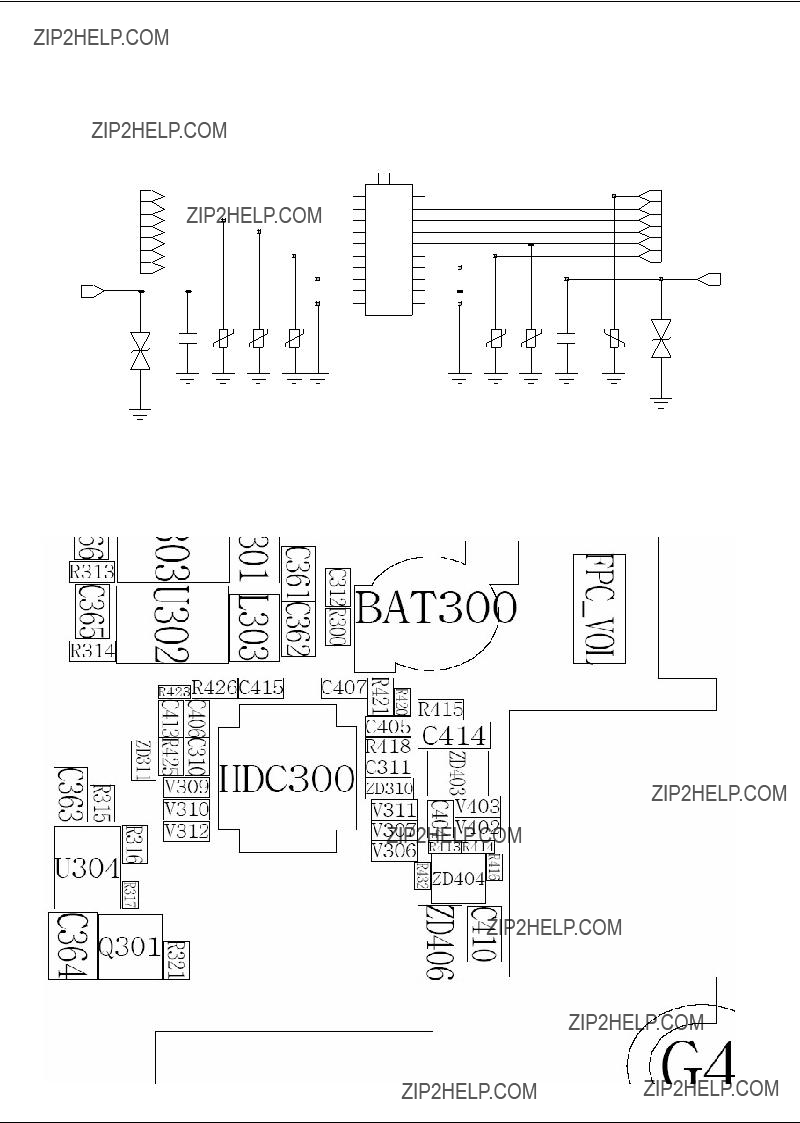
11. PCB Diagrams
U406
MAC_CPF
201TNA
G3
G4
SAMSUNG
This Document can not be used without Samsung's authorization
PCB Diagrams
TP301
ZD307
ZD308
ZD309
I CF 004
U300 U402
104
V
BTC400
SAMSUNG
This Document can not be used without Samsung's authorization

12. Block Diagrams
SAMSUNG
This Document can not be used without Samsung's authorization

13. Reference data
AAC: Advanced Audio Coding.
AVC : Advanced Video Coding.
BER : Bit Error Rate
BPSK: Binary Phase Shift Keying
CA : Conditional Access
CDM : Code Division Multiplexing
C/I : Carrier to Interference
DMB : Digital Multimedia Broadcasting
EN : European Standard
ES : Elementary Stream
ETSI: European Telecommunications Standards Institute
MPEG: Moving Picture Experts Group
PN :
PS : Pilot Symbol
QPSK: Quadrature Phase Shift Keying
RS :
SI : Service Information
TDM : Time Division Multiplexing
TS : Transport Stream
SAMSUNG
This Document can not be used without Samsung's authorization