INTEGRATED CIRCUITS
SA2411
+20 dBm single chip linear amplifier for WLAN
Supersedes data of 2002 Jul 31
P???????????????s
???????????????on????????????o???s
INTEGRATED CIRCUITS
SA2411
+20 dBm single chip linear amplifier for WLAN
Supersedes data of 2002 Jul 31
P???????????????s
???????????????on????????????o???s
1. DESCRIPTION
The SA2411 is a linear power amplifier designed for WLAN application in the 2.4 GHz band. Together with the SA2400A the chips form a complete 802.11b transceiver. The SA2411 is a Si power amplifier with integrated matching and power level detector.
2. FEATURES
???75 ?? + 25j ?? differential inputs, internally matched
???50 ??
???15 dB gain block
???Power detector
???Bias adjust pin
???18% efficiency at 3 V
???RF matching for SA2400A
3. APPLICATIONS
???IEEE 802.11 and 802.11b radios
???Supports DSSS and CCK modulation
???Supports data rates: 1, 2, 5.5, and 11 Mbps
???2.45 GHz ISM band wireless communication devices
Table 1. Ordering information
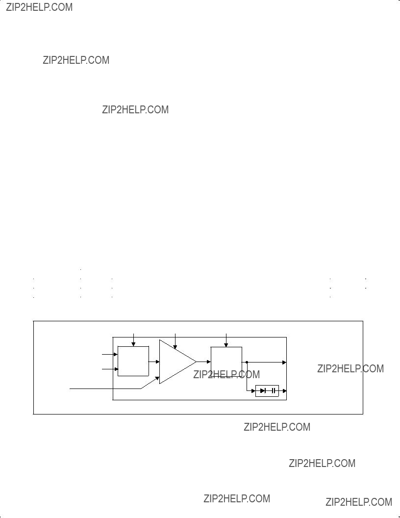
4. BLOCK DIAGRAM
VDD_DRIVERVDD_BIASVDD_MAIN
Figure 1. Block diagram

5. PINNING INFORMATION
VDD_MAIN 1 

VDD_DRIVER 2
GND 3
IN+ 4
IN?? 5
GND 6
DETECTOR 7
GND 8
Figure 2. Pin configuration
Table 2. Pin description
PIN type is designated by A = Analog, D = Digital, I = Input, O = Output
All GND pins should be connected to ground to guarantee the best performance.

6. FUNCTIONAL DESCRIPTION
The main
???Fixed gain amplifier (PA)
???Output matching
???Input matching
???Power Detector
???Power Mode
Input
The device has differential inputs so a balun is needed in the case of single ended operation, input impedance is approximately 75 ?? + 25j ??, balanced. The inputs can be DC biased with the pin VDD_DRIVER. The input matching is optimized to interface with the SA2400A WLAN transceiver chip.
Amplifier
The amplifier is a fixed gain, class AB amplifier. There is an additional pin, VDD_BIAS, to adjust the class A bias current. Reducing the class A currents reduces the gain. This allows
Output matching
The output of the amplifier is matched, on chip, for a 50 ?? load. The matching includes the supply feed for the power amplifier. The pin VDD_MAIN is the main supply for the amplifier. No additional filtering is needed to meet the 802.11b spec.
Power detector
The power detector detects the power level and transforms it into a low frequency current. The detector output must be loaded with a resistor to ground for the highest accuracy. This resistor has an optimal value of 5.6 k??. Lower values can be used to comply with maximum input sensitivity of ADCs, at the cost of dynamic range. The maximum voltage detected is 2.3 V.
Power mode
This pin selects the desired gain and linearity level (13 dB or 14.5 dB gain). The low gain is more applicable to high voltage applications from 3.3 V to 3.6 V. The high gain is more applicable to low voltage applications lower than 3.3 V.
NOTE:
In order to assure optimal thermal performance, it is recommended that all ground pins be connected, and that the number of vias to ground under the chip be maximized. In addition, the use of solder mask under the chip (for scratch protection) is not recommended.

7. CONNECTIVITY DIAGRAM
VDDPWRUP
L1
C1
L2
C2
L3
ANT
R1
SA2411
Idet.
R2
Vdet
RFin RFin
SR02385
No inductors and directly connecting all supplies to VDD might cause problems. The optimal values of the inductors depends on the application board.
8. OPERATION
The SA2411 linear amplifier is intended for operation in the 2.4 GHz band, specifically for IEEE 802.11 1 and 2 Mbits/s DSSS, and 5.5 and 11 Msymbols/s CCK standards. Throughout this document, the operating RF frequency refers to the ISM band between 2.4 and 2.5 GHz.
Amplifier Output Power
The SA2411 linear amplifier is designed to give at least 19 dBm output power for an 11 Msymbols/s CCK modulated input carrier. At 19 dBm output power the ACPR specs are met. The fixed gain amplifier amplifies the input signal by 14.5 dB typically.
Power Mode
The biasing can be adjusted to change the gain and therefore the maximum linear output power. For high supply voltages (>3.2 V) the
Power detector
The power detector current output is linear proportional with the RF output voltage. The RF output power is quadratic proportional to the RF output voltage. Therefore, the detector is quadratic proportional to the output power. The following relation can be expressed:
Pout is output power in mWatt, Vdetector is detector voltage in Volt, k = sensitivity in mWatt/V2, n = quadratic factor.
The quadratic factor is 1.5. The sensitivity is then 49 mWatt/V2.
The loading of the detector can be different in the application. The highest accuracy is achieved with 5.6 k??. But other values can be used to adapt to the maximum input sensitivity of other circuits. Other detector loading values result in other
DC feed at input
There is a possibility to add a DC voltage at the input pins (pin 4 and pin 5) by feeding pin 2. This option should be used in case the SA2411 is lined up with the SA2400A.

9. OPERATING CONDITIONS
The SA2411 shall meet all of the operating conditions outlined in this section. Table 3 specifies the absolute maximum ratings for the device. Table 4 gives the recommended operating conditions.
Table 3. Absolute maximum ratings
Table 4. Recommended operating conditions
10. SA2411 TRANSMITTER REQUIREMENTS
Table 5. SA2411 transmitter specifications
Tamb = 25 ??C; VCC = 3 V; frequency = 2.45 GHz, Rdetector = 5.6 k??, unless otherwise stated.
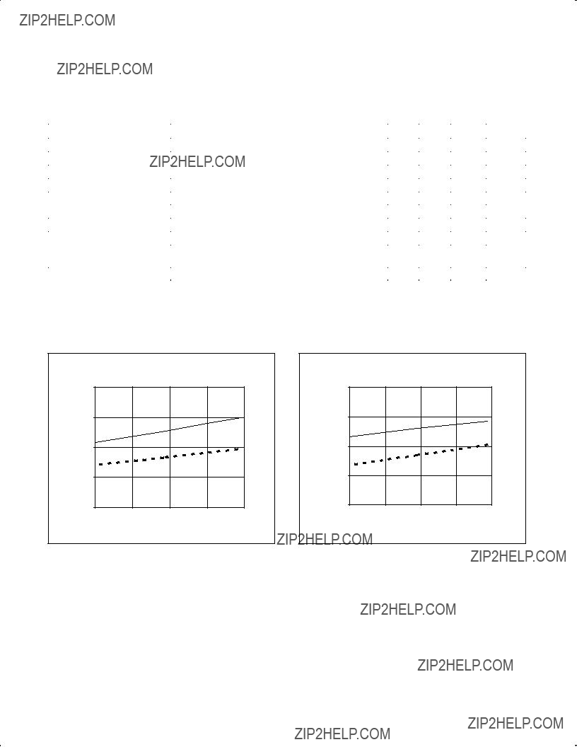
Table 6. SA2411 Detector specification
Tamb = 25 ??C, VCC = 3.0 V
11. GRAPHS
The following graphs are only for a typical sample measured on a SA2411 test board under nominal condition applying an 11Mb/s CCK 802.11b modulation. Corrections for input, output and supply losses have been applied. The dotted lines represent the low gain mode. The solid
lines are for the high gain mode.
The first two graphs are small signal graphs. The gain and the DC currents are plotted versus supply voltage.
DC current versus Supply Voltage
Gain versus Supply Voltage

The next eight graphs are presenting the power sweep for both gain modes at nominal conditions.
Output Power versus Input Power
Efficiency versus Output Power
Gain versus Output Power
Current consumption vs Output Power

ACPR versus Output Power
Figure 9. ACPR vs. output power
ALT versus Output Power
Figure 10. ALT vs. output power
Detector Voltage versus Output Power
Figure 11. Detector voltage vs. output power
Detector Error versus Output Power
Figure 12. Detector error vs. output power
The next curves present the frequency dependency for an input power of +7 dBm:
Output Power versus Frequency
Figure 13. Output power vs. frequency
Gain versus Frequency
Efficiency versus Frequency
Figure 15. Efficiency vs. frequency
ACPR versus frequency

ALT versus Frequency
Figure 17. ALT vs. frequency
Detector Voltage versus Frequency
Detector Errror versus Frequency
Figure 19. Detector error vs. frequency
Figure 18. Detector voltage vs. frequency

The last 5 curves are characterization data for supply voltage, temperature and power. The
Figure 20. DC current vs. supply voltage, mode = high
Figure 21. Gain vs. supply voltage, mode = high
Figure 22. Output power vs. supply voltage, mode = high
Figure 23. Efficiency vs. supply voltage, mode = high
Figure 24. Detector error vs. supply voltage, mode = high

12. APPLICATION WITH THE SA2400A
Next diagram is the application of the SA2400A with the SA2411.
The interface is simple. Two equal microstrip lines connect the SA2400A with the SA2411. The length of this connection should be kept to a minimum.
The supply for the open collectors of the SA2400A is provided via pin 2 of the SA2411.
C2 is for supply voltage decoupling.
VDD PWRUP
RF connection
Other connection
SA2411
Idetector
TX/RX
37
TX_IN_I_P/
TX_DATA_I
36
TX_IN_I_M/
TX_DATA_Q
35
TX_IN_Q_P
34
TX_IN_Q_M
33
SR02487
Figure 25.
NOTE: A suggested starting point for designing the coupled microstrip lines:
Length = 1/18 ??. Width = 12 mils, Separation = 5 mils with the Dielectric constant = 4.6.
This should result in Zeven = 150 ??, Zo = 75 ??, and Zodd = 30 ??.
There should be no ground plane under the microstrip lines.

REVISION HISTORY

Data sheet status
[1]Please consult the most recently issued data sheet before initiating or completing a design.
[2]The product status of the device(s) described in this data sheet may have changed since this data sheet was published. The latest information is available on the Internet at URL http://www.semiconductors.philips.com.
[3]For data sheets describing multiple type numbers, the
Definitions
Limiting values definition ?? Limiting values given are in accordance with the Absolute Maximum Rating System (IEC 60134). Stress above one or more of the limiting values may cause permanent damage to the device. These are stress ratings only and operation of the device at these or at any other conditions above those given in the Characteristics sections of the specification is not implied. Exposure to limiting values for extended periods may affect device reliability.
Application information ?? Applications that are described herein for any of these products are for illustrative purposes only. Philips Semiconductors make no representation or warranty that such applications will be suitable for the specified use without further testing or modification.
Disclaimers
Life support ?? These products are not designed for use in life support appliances, devices, or systems where malfunction of these products can reasonably be expected to result in personal injury. Philips Semiconductors customers using or selling these products for use in such applications do so at their own risk and agree to fully indemnify Philips Semiconductors for any damages resulting from such application.
Right to make changes ?? Philips Semiconductors reserves the right to make changes in the products??including circuits, standard cells, and/or software?? described or contained herein in order to improve design and/or performance. When the product is in full production (status `Production'), relevant changes will be communicated via a Customer Product/Process Change Notification (CPCN). Philips Semiconductors assumes no responsibility or liability for the use of any of these products, conveys no license or title under any patent, copyright, or mask work right to these products, and makes no representations or warranties that these products are free from patent, copyright, or mask work right infringement, unless otherwise specified.
Contact information
For sales offices addresses send
sales.addresses@www.semiconductors.philips.com.
??? Koninklijke Philips Electronics N.V. 2003 All rights reserved. Printed in U.S.A.
Date of release:
P???????????????s
???????????????on????????????o???s