Professional Radio
GP Series
300R1 (300 - 350MHz)
Service Information
Issue: June 2002
Professional Radio
GP Series
300R1 (300 - 350MHz)
Service Information
Issue: June 2002

ii
Computer Software Copyrights
The Motorola products described in this manual may include copyrighted Motorola computer programs stored in semiconductor memories or other media. Laws in the United States and other countries preserve for Motorola certain exclusive rights for copyrighted computer programs, including the exclusive right to copy or reproduce in any form, the copyrighted computer program. Accordingly, any copyrighted Motorola computer programs contained in the Motorola products described in this manual may not be copied or reproduced in any manner without the express written permission of Motorola. Furthermore, the purchase of Motorola products shall not be deemed to grant, either directly or by implication, estoppel or otherwise, any license under the copyrights, patents or patent applications of Motorola, except for the normal

iii
Table of Contents

iv
Chapter 1
MODEL CHART AND TECHNICAL SPECIFICATIONS
1.0GP340 Model Chart
Professional GP300 Series
x = Indicates one of each is required.
2.0GP640 / GP680 Model Chart
Professional GP600 Series
x = Indicates one of each is required.

*Availability subject to the laws and regulations of individual countries.

Chapter 2
THEORY OF OPERATION
1.0Introduction
This Chapter provides a detailed theory of operation for the
2.0Transmitter
(Refer to Figure
The transmitter contains five basic circuits:
1.power amplifier,
2.antenna switch,
3.harmonic filter,
4.antenna matching network,
5.power control integrated circuit (PCIC).
Figure
2.1Power Amplifier
The power amplifier consists of two devices:
1.9Z67 LDMOS driver IC (U101) and
2.PRF1507 LDMOS PA (Q110).
The 9Z67 LDMOS driver IC contains 2 stages of amplification with a supply voltage of 7.3V.
This RF power amplifier is capable of supplying an output power of 0.3W (pin 6 and 7) with an input signal of 2mW (3dBm) (pin16). The current drain would typically be 160mA while operating in the frequency range of
The PRF1507 LDMOS PA is capable of supplying an output power of 7W with an input signal of 0.3W. The current drain would typically be 1300mA while operating in the frequency range of
2.2Antenna Switch
The antenna switch circuit consists of two PIN diodes (CR101 and CR102), a pi network (C107, L104 and C106), and two current limiting resistors (R101, R170). In the transmit mode, B+ at PCIC (U102) pin 23 will go low and turn on Q111 where a B+ bias is applied to the antenna switch circuit to bias the diodes "on". The shunt diode (CR102) shorts out the receiver port, and the pi network, which operates as a quarter wave transmission line, transforms the low impedance of the shunt diode to a high impedance at the input of the harmonic filter. In the receive mode, the diodes are both off, and hence, there exists a low attenuation path between the antenna and receiver ports.
2.3Harmonic Filter
The harmonic filter consists of C104, L102, C103, L101 and C102. The design of the harmonic filter for VHF is that of a modified Zolotarev design. It has been optimized for efficiency of the power module. This type of filter has the advantage that it can give a greater attenuation in the
2.4Antenna Matching Network
A matching network which is made up of L116 is used to match the antenna's impedance to the harmonic filter. This will optimize the performance of the transmitter and receiver into an antenna.
2.5Power Control Integrated Circuit (PCIC)
The transmitter uses the Power Control IC (PCIC), U102 to regulate the power output of the radio. The current to the final stage of the power module is supplied through R101, which provides a voltage proportional to the current drain. This voltage is then fedback to the Automatic Level Control (ALC) within the PCIC to regulate the output power of the transmitter.
The PCIC has internal digital to analog converters (DACs) which provide the reference voltage of the control loop. The reference voltage level is programmable through the SPI line of the PCIC.
There are resistors and integrators within the PCIC, and external capacitors (C133, C134 and C135) in controlling the transmitter rising and falling time. These are necessary in reducing the power splatter into adjacent channels.
CR105 and its associated components are part of the temperature cut back circuitry. It senses the printed circuit board temperature around the transmitter circuits and output a DC voltage to the PCIC. If the DC voltage produced exceeds the set threshold in the PCIC, the transmitter output power will be reduced so as to reduce the transmitter temperature.
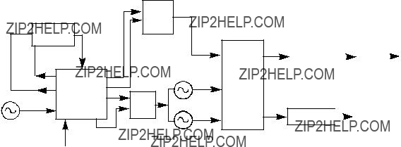
3.0Receiver
Control Voltage from ASFIC
AGC
First LO from FGU
16.8 MHz
Reference Clock
SPI Bus
Second
LO VCO
Figure
3.1Receiver
(Refer to Figure
The RF signal is received by the antenna and applied to a
The bandpass filter is electronically tuned by the DACRx from U404 which is controlled by the microprocessor. Depending on the carrier frequency, the DACRx will supply the tuned voltage to the varactor diodes in the filter. Wideband operation of the filter is achieved by shifting the bandpass filter across the band.
The output of the bandpass filter is coupled to the RF amplifier transistor Q301 via C307. After being amplified by the RF amplifier, the RF signal is further filtered by a second varactor tuned bandpass filter, consisting of L306, L307, C313, C317, CR304 and CR305.
Both the pre and
The output of the
The IF signal coming out of the mixer is transfered to the crystal filter (FL301) through a resistor pad and a diplexer (C322 and L310). Matching to the input of the crystal filter is provided by C324 and L311. The crystal filter provides the necessary selectivity and intermodulation protection.
3.2Receiver
(Refer to Figure
The output of crystal filter FL301 is matched to the input of IF amplifier transistor Q302 by components R352 and C325. Voltage supply to the IF amplifier is taken from the receive 5 volts (R5). The IF amplifer provides a gain of about 7dB. The amplified IF signal is then coupled into U301(pin 3) via C330, C338 and L330 which provides the matching for the IF amplifier and U301.
The IF signal applied to pin 3 of U301 is amplified,
The IF IC uses a type of direct conversion process, whereby the externally generated second LO frequency is divided by two in U301 so that it is very close to the first IF frequency. The IF IC (U301) synthesizes the second LO and
In the absence of an IF signal, the VCO will ???search??? for a frequency, or its frequency will vary close to twice the IF frequency. When an IF signal is received, the VCO will lock onto the IF signal. The second LO/VCO is a Colpitts oscillator built around transistor Q320. The VCO has a varactor diode, CR310, to adjust the VCO frequency. The control signal for the varactor is derived from a loop filter consisting of C362, C363, C364, R320 and R321.
The IF IC (U301) also performs several other functions. It provides a received
The demodulated signal on pin 27 of U301 is also used for squelch control. The signal is routed to U404 (ASFIC) where squelch signal shaping and detection takes place. The demodulated audio signal is also routed to U404 for processing before going to the audio amplifier for amplification.
3.3Automatic Gain Control Circuit
(Refer to the Receiver Front End and Receiver Back End schematic diagrams)
The front end automatic gain control circuit is to provide automatic gain reduction of the front end RF amplifier via feedback. This action is necessary to prevent overloading of backend circuits. This is achieved by drawing some of the output power from the RF amplifier???s output. At high radio frequencies, capacitor C331 provides the low impedance path to ground for this purpose. CR308 is a PIN diode used for switching the path on or off. A certain amount of forward biasing current is needed to turn the PIN diode on. Transistors Q315 provides this current where upon saturation, current will flow via R347, PIN diode, collector and emitter of Q315 and R319 before going to ground. Q315 is an NPN transistor used for switching here. Maximum current flowing through the PIN is mainly limited by the resistor R319.
Radio signal strength indicator, RSSI, a voltage signal, is used to drive Q315 to saturation hence turning it on. RSSI is produced by U301 and is proportional to the gain of the RF amplifier and the input RF signal power to the radio.
Resistor network at the input to the base of Q315 is scaled to turn on Q315, hence activating the AGC, at certain RSSI levels. In order to turn on Q315, the voltage across the transistor???s base to ground must be greater or equal to the voltage across R319, plus the
4.0Frequency Generation Circuitry
(Refer to Figure
The Frequency Generation Circuitry is composed of two main ICs, the
Modulating
Signal
Figure
The synthesizer is powered by regulated 5V and 3.3V which come from U247 and U248 respectively. The synthesizer in turn generates a superfiltered 4.5V which powers U241.
In addition to the VCO, the synthesizer must interface with the logic and ASFIC circuitry. Programming for the synthesizer is accomplished through the data , clock and chip select lines from the microprocessor. A 3.3V dc signal from synthesizer lock detect line indicates to the microprocessor that the synthesizer is locked.
Transmit modulation from the ASFIC is supplied to pin10 of U201. Internally the audio is digitized by the
4.1Synthesizer
(Refer to Figure
The
The loop filter which consist of C231, C232, C233, R231, R232 and R233 provides the necessary dc steering voltage for the VCO and determines the amount of noise and spur passing through.

In achieving fast locking for the synthesizer, an internal adapt charge pump provides higher current at pin 45 of U201 to put synthesizer within the lock range. The required frequency is then locked by normal mode charge pump at pin 43 .
Both the normal and adapt charge pumps get their supply from the capacitive voltage multiplier which is made up of C258, C259, C228, triple diode CR201 and level shifters U210 and U211. Two 3.3V square waves (180 deg out of phase) are first shifted to 5V, then along with regulated 5V , put through arrays of diodes and capacitors to build up 13.3V at pin 47 of U201.
Figure
4.2Voltage Controlled Oscillator (VCO)
(Refer to Figure
The VCOBIC (U241) in conjunction with the
The VCOBIC(U241) is operated at 4.54 V (VSF) and
The operation logic is shown in Table
Figure
Table
In the receive mode, U241 pin 19 is low or grounded. This activates the receive VCO by enabling the receive oscillator and the receive buffer of U241. The RF signal at U241 pin 8 is run through a matching network. The resulting RF signal is the LO RF INJECTION and it is applied to the mixer at T302.
During the transmit condition, when PTT is depressed, five volts is applied to U241 pin 19. This activates the transmit VCO by enabling the transmit oscillator and the transmit buffer of U241. The RF signal at U241 pin 10 is injected into the input of the PA module (U101 pin16). This RF signal is the TX RF INJECTION. Also in transmit mode, the audio signal to be frequency modulated onto the carrier is received through the U201 pin 41.
When a high impedance is applied to U241 pin19, the VCO is operating in BATTERY SAVER mode. In this case, both the receive and transmit oscillators as well as the receive transmit and prescaler buffer are turned off.

Chapter 3
TROUBLESHOOTING CHARTS
1.0Troubleshooting Flow Chart for Receiver (Sheet 1 of 2)
START
Bad SINAD
Bad 20dB Quieting
No Recovered Audio
No
Spray of inject 1st IF into
XTAL Filter
IF Freq: 45.1MHz
No
Check 2nd LO Control Voltage at C363
Yes VCO
B 
 locked?
Check Controller
A
Check Q320 bias circuitry for faults.
Rotate Freq. Knob
Yes
Check controller
Before replacing U301, check 2nd
VCO Q320. Check VCO O/P level,
C351, C352.
No
Check FGU
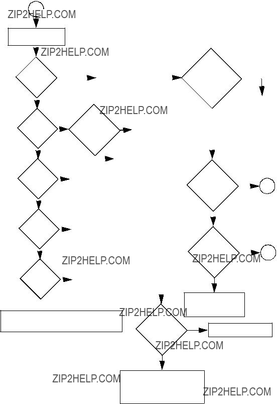
2.0Troubleshooting Flow Chart for Receiver (Sheet 2 of 2)
B 
Inject RF into J101
No or  weak RF
No 
Check harmonic filters L101 & L102
and ant. switches CR101, CR102, L104 Are varactor voltages OK?
No
Check Q210, U201 (pin
48) voltages
and U247
Yes
Check varactor filter.
No
Check U404 voltage. U404 can be selected by MCU before replacing U404.
3.0Troubleshooting Flow Chart for Transmitter
START
No Power
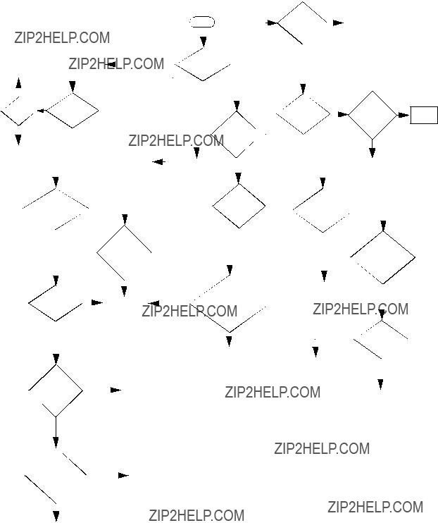
4.0Troubleshooting Flow Chart for Synthesizer
YES
Replace
U201
5.0Troubleshooting Flow Chart for VCO
Yes
Change
L253
START
Yes
No
No
Check U201
Pin 2 for 3.2V
VCTRL Yes 0V or
13V?
No
Check for faulty parts or dry joints of L271, L273, C370, C386, R339 & L320
Circuit?L243
No
Change
U241
No
Change
U201
Chapter 4
PCB/SCHEMATICS/PARTS LISTS
1.0Allocation of Schematics and Circuit Boards
1.1Controller Circuits
The
Table
Table