PENT/ATCA???717
Reference Guide
P/N 6806800A15A
April 2006
PENT/ATCA???717
Reference Guide
P/N 6806800A15A
April 2006

Copyright
ECopyright 2006 Motorola GmbH
All rights reserved.
Motorola and the stylized M logo are trademarks of Motorola,Inc., registered in the U.S. Patent and Trademark Office.
All other product or service names mentioned in this document are the property of their respective owners.
Notice
While reasonable efforts have been made to assure the accuracy of this document, Motorola GmbH assumes no liability resulting from any ommissions in this document, or from the use of the information obtained herein. Motorola reserves the right to revise this document and to make changes from time to time in the content hereof without obligation of Motorola to notify any person of such revision or changes.
Electronic versions of this material may be read online, downloaded for personal use, or referenced in another document as a URL to the Motorola Embedded Communications Computing Web site. The text itself may not be published commercially in print or electronic form, edited, translated, or otherwise altered without the permission of Motorola GmbH.
It is possible that this publication may contain reference to or information about Motorola products (machines and programs), programming, or services that are not available in your country. Such references or information must not be construed to mean that Motorola intends to announce such Motorola products, programming, or services in your country.

Contents


Tables
Introduction
Tablei1aaaaaaaOrganization of this Manual . . . . . . . . . . . . . . . . . . . . . . . . . . . . . . . . . . . . . . . . . . . . . . . . . . . . . . . 29 Tablei2aaaaaaaOrdering Information . . . . . . . . . . . . . . . . . . . . . . . . . . . . . . . . . . . . . . . . . . . . . . . . . . . . . . . . . . . . . 33 Tablei3aaaaaaaAccessories Ordering Information . . . . . . . . . . . . . . . . . . . . . . . . . . . . . . . . . . . . . . . . . . . . . . . . . . 33
Installation
Tablei4aaaaaaaEnvironmental Requirements . . . . . . . . . . . . . . . . . . . . . . . . . . . . . . . . . . . . . . . . . . . . . . . . . . . . . . 37
Tablei5aaaaaaaPower Requirements . . . . . . . . . . . . . . . . . . . . . . . . . . . . . . . . . . . . . . . . . . . . . . . . . . . . . . . . . . . . . 40
Tablei6aaaaaaaSwitch Settings . . . . . . . . . . . . . . . . . . . . . . . . . . . . . . . . . . . . . . . . . . . . . . . . . . . . . . . . . . . . . . . . . . 43
Controls, Indicators, and Connectors
Tablei7aaaaaaaFace Plate LEDs . . . . . . . . . . . . . . . . . . . . . . . . . . . . . . . . . . . . . . . . . . . . . . . . . . . . . . . . . . . . . . . . . 60
BIOS
Tablei8aaaaaaaKey Codes for Terminal Emulation Program . . . . . . . . . . . . . . . . . . . . . . . . . . . . . . . . . . . . . . . . . 84 Tablei9aaaaaaaStandard BIOS Post Codes . . . . . . . . . . . . . . . . . . . . . . . . . . . . . . . . . . . . . . . . . . . . . . . . . . . . . . . 96
Devices??? Features and Data Paths
Tablei10aaaaaaReset Sources . . . . . . . . . . . . . . . . . . . . . . . . . . . . . . . . . . . . . . . . . . . . . . . . . . . . . . . . . . . . . . . . . . 117 Tablei11aaaaaaOn???board Sensors Accessible via IPMI . . . . . . . . . . . . . . . . . . . . . . . . . . . . . . . . . . . . . . . . . . . . 121 Tablei12aaaaaaEthernet Switching Unit ???Ethernet Port Distribution . . . . . . . . . . . . . . . . . . . . . . . . . . . . . . . . . . 129 Tablei13aaaaaaEthernet Switching Unit ??? Port Assignment . . . . . . . . . . . . . . . . . . . . . . . . . . . . . . . . . . . . . . . . . 131
Maps and Registers
Tablei14aaaaaaMemory Address Map . . . . . . . . . . . . . . . . . . . . . . . . . . . . . . . . . . . . . . . . . . . . . . . . . . . . . . . . . . . 133 Tablei15aaaaaaI/O Address Map . . . . . . . . . . . . . . . . . . . . . . . . . . . . . . . . . . . . . . . . . . . . . . . . . . . . . . . . . . . . . . . . 133 Tablei16aaaaaaHardware Interrupts . . . . . . . . . . . . . . . . . . . . . . . . . . . . . . . . . . . . . . . . . . . . . . . . . . . . . . . . . . . . . 135 Tablei17aaaaaaPCI Device Interrupts . . . . . . . . . . . . . . . . . . . . . . . . . . . . . . . . . . . . . . . . . . . . . . . . . . . . . . . . . . . . 136 Tablei18aaaaaaRegisters Accessible from CPU via LPC Bus . . . . . . . . . . . . . . . . . . . . . . . . . . . . . . . . . . . . . . . 137 Tablei19aaaaaaIndex Addresses of Registers Accessible from CPU via LPC Bus . . . . . . . . . . . . . . . . . . . . . . 137 Tablei20aaaaaaIPMI Block Transfer Interface Registers . . . . . . . . . . . . . . . . . . . . . . . . . . . . . . . . . . . . . . . . . . . . 138 Tablei21aaaaaaEthernet Switch Management Registers . . . . . . . . . . . . . . . . . . . . . . . . . . . . . . . . . . . . . . . . . . . . 138 Tablei22aaaaaaCommand and Status Register . . . . . . . . . . . . . . . . . . . . . . . . . . . . . . . . . . . . . . . . . . . . . . . . . . . 139 Tablei23aaaaaaReset Source Register . . . . . . . . . . . . . . . . . . . . . . . . . . . . . . . . . . . . . . . . . . . . . . . . . . . . . . . . . . . 140 Tablei24aaaaaaReset Mask Register . . . . . . . . . . . . . . . . . . . . . . . . . . . . . . . . . . . . . . . . . . . . . . . . . . . . . . . . . . . . 140 Tablei25aaaaaaMiscellaneous Switch Status Register . . . . . . . . . . . . . . . . . . . . . . . . . . . . . . . . . . . . . . . . . . . . . 141 Tablei26aaaaaaLED Control Register . . . . . . . . . . . . . . . . . . . . . . . . . . . . . . . . . . . . . . . . . . . . . . . . . . . . . . . . . . . . 142 Tablei27aaaaaaPMC Status Register . . . . . . . . . . . . . . . . . . . . . . . . . . . . . . . . . . . . . . . . . . . . . . . . . . . . . . . . . . . . 143 Tablei28aaaaaaClock Synchronisation Interface Registers . . . . . . . . . . . . . . . . . . . . . . . . . . . . . . . . . . . . . . . . . . 144 Tablei29aaaaaaDPLL Input Select and Control Register . . . . . . . . . . . . . . . . . . . . . . . . . . . . . . . . . . . . . . . . . . . . 145 Tablei30aaaaaaReference Clock Source Register . . . . . . . . . . . . . . . . . . . . . . . . . . . . . . . . . . . . . . . . . . . . . . . . . 145 Tablei31aaaaaaExamples of Division Factors Between Recovered and Reference Clock . . . . . . . . . . . . . . . 146 Tablei32aaaaaaLower Divider Register . . . . . . . . . . . . . . . . . . . . . . . . . . . . . . . . . . . . . . . . . . . . . . . . . . . . . . . . . . . 147

Tablei33aaaaaaUpper Divider Register . . . . . . . . . . . . . . . . . . . . . . . . . . . . . . . . . . . . . . . . . . . . . . . . . . . . . . . . . . . 147
Tablei34aaaaaaReference Clock Pulse Width Register . . . . . . . . . . . . . . . . . . . . . . . . . . . . . . . . . . . . . . . . . . . . . 147
Tablei35aaaaaaVersion Register . . . . . . . . . . . . . . . . . . . . . . . . . . . . . . . . . . . . . . . . . . . . . . . . . . . . . . . . . . . . . . . . 148
Tablei36aaaaaaAccess Control Register . . . . . . . . . . . . . . . . . . . . . . . . . . . . . . . . . . . . . . . . . . . . . . . . . . . . . . . . . 148

Figures
Installation
Figurei1aaaaaaaLocation of Critical Blade Temperature Spots (Blade Top Side) . . . . . . . . . . . . . . . . . . . . . . . . 39 Figurei2aaaaaaaLocation of Critical Blade Temperature Spots (Blade Bottom Side) . . . . . . . . . . . . . . . . . . . . . 40 Figurei3aaaaaaaLocation of On???board Switches . . . . . . . . . . . . . . . . . . . . . . . . . . . . . . . . . . . . . . . . . . . . . . . . . . . 42 Figurei4aaaaaaaLocation of PMC Slots . . . . . . . . . . . . . . . . . . . . . . . . . . . . . . . . . . . . . . . . . . . . . . . . . . . . . . . . . . . 47 Figurei5aaaaaaaLocation of On???Board Hard Disk . . . . . . . . . . . . . . . . . . . . . . . . . . . . . . . . . . . . . . . . . . . . . . . . . . 49 Figurei6aaaaaaaLocation of CompactFlash Disk Connector . . . . . . . . . . . . . . . . . . . . . . . . . . . . . . . . . . . . . . . . . 51
Controls, Indicators, and Connectors
Figurei7aaaaaaaFace Plate . . . . . . . . . . . . . . . . . . . . . . . . . . . . . . . . . . . . . . . . . . . . . . . . . . . . . . . . . . . . . . . . . . . . . 59 Figurei8aaaaaaaLocation of Face Plate LEDs . . . . . . . . . . . . . . . . . . . . . . . . . . . . . . . . . . . . . . . . . . . . . . . . . . . . . . 60 Figurei9aaaaaaaLocation of Reset Key . . . . . . . . . . . . . . . . . . . . . . . . . . . . . . . . . . . . . . . . . . . . . . . . . . . . . . . . . . . 62 Figurei10aaaaaaLocation of USB Connectors . . . . . . . . . . . . . . . . . . . . . . . . . . . . . . . . . . . . . . . . . . . . . . . . . . . . . . 63 Figurei11aaaaaaFace Plate USB Connector Pinout . . . . . . . . . . . . . . . . . . . . . . . . . . . . . . . . . . . . . . . . . . . . . . . . . 63 Figurei12aaaaaaLocation of PMC Connectors Pn1 to Pn4 . . . . . . . . . . . . . . . . . . . . . . . . . . . . . . . . . . . . . . . . . . . 65 Figurei13aaaaaaPMC Sites 1 and 4 ??? Pn4 Connector Pinout . . . . . . . . . . . . . . . . . . . . . . . . . . . . . . . . . . . . . . . . 66 Figurei14aaaaaaPMC Sites 2 and 3 ??? Pn4 Connector Pinout . . . . . . . . . . . . . . . . . . . . . . . . . . . . . . . . . . . . . . . . 67 Figurei15aaaaaaLocation of Parallel ATA Connector . . . . . . . . . . . . . . . . . . . . . . . . . . . . . . . . . . . . . . . . . . . . . . . . 68 Figurei16aaaaaaParallel ATA Connector Pinout . . . . . . . . . . . . . . . . . . . . . . . . . . . . . . . . . . . . . . . . . . . . . . . . . . . . 69 Figurei17aaaaaaLocation of Serial ATA Connector . . . . . . . . . . . . . . . . . . . . . . . . . . . . . . . . . . . . . . . . . . . . . . . . . . 70 Figurei18aaaaaaLocation of CMC Connector . . . . . . . . . . . . . . . . . . . . . . . . . . . . . . . . . . . . . . . . . . . . . . . . . . . . . . 72 Figurei19aaaaaaP10 Backplane Connector Pinout . . . . . . . . . . . . . . . . . . . . . . . . . . . . . . . . . . . . . . . . . . . . . . . . . 75 Figurei20aaaaaaP20 Backplane Connector Pinout ??? Rows A to D . . . . . . . . . . . . . . . . . . . . . . . . . . . . . . . . . . . . 76 Figurei21aaaaaaP20 Backplane Connector Pinout ??? Rows E to H . . . . . . . . . . . . . . . . . . . . . . . . . . . . . . . . . . . . 76 Figurei22aaaaaaP22 Backplane Connector Pinout ??? Rows A to D . . . . . . . . . . . . . . . . . . . . . . . . . . . . . . . . . . . . 76 Figurei23aaaaaaP22 Backplane Connector Pinout ??? Rows E to H . . . . . . . . . . . . . . . . . . . . . . . . . . . . . . . . . . . . 77 Figurei24aaaaaaP23 Backplane Connector Pinout ??? Rows A to D . . . . . . . . . . . . . . . . . . . . . . . . . . . . . . . . . . . . 77 Figurei25aaaaaaP23 Backplane Connector Pinout ??? Rows E to H . . . . . . . . . . . . . . . . . . . . . . . . . . . . . . . . . . . . 77 Figurei26aaaaaaP30 Backplane Connector Pinout ??? Rows A to D . . . . . . . . . . . . . . . . . . . . . . . . . . . . . . . . . . . . 78 Figurei27aaaaaaP30 Backplane Connector Pinout ??? Rows E to H . . . . . . . . . . . . . . . . . . . . . . . . . . . . . . . . . . . . 78 Figurei28aaaaaaP31 Backplane Connector Pinout ??? Rows A to D . . . . . . . . . . . . . . . . . . . . . . . . . . . . . . . . . . . . 79 Figurei29aaaaaaP31 Backplane Connector Pinout ??? Rows E to H . . . . . . . . . . . . . . . . . . . . . . . . . . . . . . . . . . . . 79 Figurei30aaaaaaP32 Backplane Connector Pinout ??? Rows A to D . . . . . . . . . . . . . . . . . . . . . . . . . . . . . . . . . . . . 79 Figurei31aaaaaaP32 Backplane Connector Pinout ??? Rows E to H . . . . . . . . . . . . . . . . . . . . . . . . . . . . . . . . . . . . 80
BIOS
Figurei32aaaaaaMain Menu . . . . . . . . . . . . . . . . . . . . . . . . . . . . . . . . . . . . . . . . . . . . . . . . . . . . . . . . . . . . . . . . . . . . . 87
Figurei33aaaaaaBoot Menu . . . . . . . . . . . . . . . . . . . . . . . . . . . . . . . . . . . . . . . . . . . . . . . . . . . . . . . . . . . . . . . . . . . . . 90
Devices??? Features and Data Paths
Figurei34aaaaaaBase Board Block Diagram . . . . . . . . . . . . . . . . . . . . . . . . . . . . . . . . . . . . . . . . . . . . . . . . . . . . . . 105
Figurei35aaaaaaBoot Flash LPC Device ID Control . . . . . . . . . . . . . . . . . . . . . . . . . . . . . . . . . . . . . . . . . . . . . . . . 113
Figurei36aaaaaaIPMI Structure . . . . . . . . . . . . . . . . . . . . . . . . . . . . . . . . . . . . . . . . . . . . . . . . . . . . . . . . . . . . . . . . . 119
Figurei37aaaaaaIPMI Temperature Sensors . . . . . . . . . . . . . . . . . . . . . . . . . . . . . . . . . . . . . . . . . . . . . . . . . . . . . . 120
Figurei38aaaaaaClock Synchronization Building Block . . . . . . . . . . . . . . . . . . . . . . . . . . . . . . . . . . . . . . . . . . . . . 124
Figurei39aaaaaaBlade Power Supply Structure . . . . . . . . . . . . . . . . . . . . . . . . . . . . . . . . . . . . . . . . . . . . . . . . . . . 126
Figurei40aaaaaaVLAN Configuration . . . . . . . . . . . . . . . . . . . . . . . . . . . . . . . . . . . . . . . . . . . . . . . . . . . . . . . . . . . . 130
Maps and Registers
Figurei41aaaaaaPCI Structure . . . . . . . . . . . . . . . . . . . . . . . . . . . . . . . . . . . . . . . . . . . . . . . . . . . . . . . . . . . . . . . . . . 136
Battery Exchange
Figurei42aaaaaaLocation of On???board Battery . . . . . . . . . . . . . . . . . . . . . . . . . . . . . . . . . . . . . . . . . . . . . . . . . . . . 152

Using This Guide
This Reference Guide is intended for users qualified in electronics or electrical engineering. Users must have a working understanding of Peripheral Component Interconnect (PCI), AdvancedTCAR, and telecommunications.
Conventions
Possibly dangerous situation: slight injuries to people or damage to objects possible

Abbreviations


Revision History
description of redundant BIOS feature

Motorola;generalized safety notes regarding maximum combined power dissipation of installed PMC modules; in power requirements: added exceptions applicable to US and Canada; in standard compliances: removed IEC60068 (officially withdrawn) and UL94V???0/1 (already covered by 60950 and NEBS) standard; added section "Restoring BIOS Default Settings"; added "Restore BIOS Default Settings" procedure; added info on redundant FPGA feature (section Devices Features and Datapaths???>FPGA); in switch setting description and Flashes section: renamed boot flash to default flash and user flash to backup flash; extended description of redundant flash feature; in standard compliances section: added note on NEBS compliance and grounding; adapted figures showing the blade face plate to new Motorola face plate; added note to section "Updating BIOS"; updated list of IPMI sensors in section: Intelligent Platform Management Controller
in section "Switch Settings" extended description of "Clear CMOS RAM" and "Serial COM port swapping" switch ; extended section BIOS???>Serial Console Redirect???>Default Configuration; added section "About this Manual"

parallel ATA connector pinout; modified description of on???board switches SW4???1, SW4???2 and SW4???4 (default settings were changed); updated description of Ethernet switch configuration (new routing); updated PMC Pn4 pinout description; extended description of face plate LEDs; updated description of P23 backplane connector pinout; added section: BIOS???>Crisis Recovery Mode; updated on???board switch description: crisis recovery switch no more reserved;changed location of two temperature sensors and adapted list of IPMI sensors; removed references to full mesh routing: no longer an available option; in blade installation: removed warning regarding plastic handles (new handles are used now); updated ordering information

Other Sources of Information
For further information refer to the following documents.a
Note:aCheck the Motorola literature catalog for errata sheets that may be applicable to the blade.a


Safety Notes
This section provides safety precautions to follow when installing, operating, and maintaining the product.
We intend to provide all necessary information to install and handle the product in this manual. However, as the product is complex and its usage manifold, we do not guarantee that the given information is complete. If you need additional information, ask your Motorola representative.
The product has been designed to meet the standard industrial safety requirements. It must not be used except in its specific area of office telecommunication industry and industrial control.
Only personnel trained by Motorola or persons qualified in electronics or electrical engineering are authorized to install, remove or maintain the product. The information given in this manual is meant to complete the knowledge of a specialist and must not be taken as replacement for qualified personnel.
EMC
The blade has been tested in a standard Motorola system and found to comply with the limits for a Class A digital device in this system, pursuant to part 15 of the FCC Rules, EN 55022 Class A respectively. These limits are designed to provide reasonable protection against harmful interference when the system is operated in a commercial environment.
The blade generates and uses radio frequency energy and, if not installed properly and used in accordance with this guide, may cause harmful interference to radio communications. Operating the system in a residential area is likely to cause harmful interference, in which case the user will be required to correct the interference at his own expense.
Installation
Damage of Circuits
Electrostatic discharge and incorrect blade installation and removal can damage circuits or shorten their life.
Before touching the blade or electronic components, make sure that you are working in an ESD???safe environment.
Data loss
Removing the blade with the blue LED still blinking causes data loss.
Wait until the blue LED is permanently illuminated, before removing the blade.
Damage of Blade and Additional Devices and Modules
Incorrect installation of additional devices or modules may damage the blade or the additional devices or modules.
Before installing or removing an additional device or module, read the respective documentation
Operation
Blade damage Blade surface
High humidity and condensation on the blade surface causes short circuits.
Do not operate the blade outside the specified environmental limits. Make sure the blade is completely dry and there is no moisture on any surface before applying power. Do not operate the blade below 0??C.
Blade Overheating and Blade Damage
Operating the blade without forced air cooling may lead to blade overheating and thus blade damage.
When operating the blade, make sure that forced air cooling is available in the shelf.
When operating the blade in areas of electromagnetic radiation ensure that the blade is bolted on the system and the system is shielded by enclosure.
Injuries or short circuits Blade or power supply
In case the ORing diodes of the blade fail, the blade may trigger a short circuit between input line A and input line B so that line A remains powered even if it is disconnected from the power supply circuit (and vice versa).
To avoid damage or injuries, always check that there is no more voltage on the line that has been disconnected before continuing your work.
Switch Settings
Blade Malfunction
Switches marked as ???reserved??? might carry production???related functions and can cause the blade to malfunction if their setting is changed.
Therefore, do not change settings of switches marked as ???reserved???. The setting of switches which are not marked as ???reserved??? has to be checked and changed before blade installation.
Blade Damage
Setting/resetting the switches during operation can cause blade damage. Therefore, check and change switch settings before you install the blade.

Environment
Always dispose of used blades according to your country???s legislation, if possible in an environmentally acceptable way.
PMC Modules
Limited Power on PMC Modules and RTMs
The blade does not provide an extra fuse for PMC modules and RTMs.
PMC modules and RTMs used together with the blade have to be qualified according to the following standards: IEC 60950???1, EN 60950???1, UL 60950???1, CAN/CSA C22???2 No 60950???1
Excession of blade???s power consumption
Exceeding the maximum combined power dissipation of installed PMC modules may damage the blade.a
Make sure that the combined power dissipation of installed PMC modules on the 3.3V and 5V rail does not exceed 60W.
PMC Module Malfunctioning
Processor PMC modules (as defined in ANSI/VITA 32???2003) can be operated in two different modes: monarch and non???monarch mode.a
Make sure to operate any installed processor PMC modules (as defined in ANSI/VITA 32???2003) only in non???monarch mode.a
Damage of Installed Hard Disk
If PPMC/270 or PPMC/280 modules are installed into PMC slot 1 or 2, the heat radiated by the heat sink of theses PMC modules heats up an installed hard disk that may be installed at the same time.a
If PPMC/270 or PPMC/280 modules are installed into PMC slot 1 or 2, make sure not to have a hard disk installed at the same time.a
Battery
Blade/System damage
Incorrect exchange of lithium batteries can result in a hazardous explosion.a Therefore, exchange the battery as described in this manual.
Data loss
If the battery does not provide enough power anymore, the RTC is initialized and the data in the NVRAM is lost.
Therefore, exchange the battery before seven years of actual battery use have elapsed.

Data loss
Exchanging the battery always results in data loss of the devices which use the battery as power backup.a
Therefore, back up affected data before exchanging the battery.
Data loss
If installing another battery type than is mounted at blade delivery may cause data loss since other battery types may be specified for other environments or may have a shorter lifetime.
Therefore, only use the same type of lithium battery as is already installed.

Sicherheitshinweise
Dieser Abschnitt enth??lt Sicherheitshinweise, die bei Installation, Betrieb und Wartung des Produkts zu beachten sind.
Wir sind darauf bedacht, alle notwendigen Informationen, die f??r die Installation und den Betrieb erforderlich sind, in diesem Handbuch bereit zu stellen. Da es sich jedoch um ein komplexes Produkt mit vielf??ltigen Einsatzm??glichkeiten handelt, k??nnen wir die Vollst??ndigkeit der im Handbuch enthaltenen Informationen nicht garantieren. Falls Sie weitere Informationen ben??tigen sollten, wenden Sie sich bitte an die f??r Sie zust??ndige Gesch??ftsstelle von Motorola.
Das Produkt erf??llt die f??r die Industrie geforderten Sicherheitsvorschriften und darf ausschlie??lich f??r Anwendungen in der Telekommunikationsindustrie und im Zusammenhang mit Industriesteuerungen verwendet werden.
Installation, Wartung und Betrieb d??rfen nur von durch Motorola ausgebildetem oder im Bereich Elektronik oder Elektrotechnik qualifiziertem Personal durchgef??hrt werden. Die in diesem Handbuch enthaltenen Informationen dienen ausschlie??lich dazu, das Wissen von Fachpersonal zu erg??nzen, k??nnen es aber in keinem Fall ersetzen.
EMV
Das Blade wurde in einem Motorola Standardsystem getestet. Es erf??llt die f??r digitale Ger??te der Klasse A g??ltigen Grenzwerte in einem solchen System gem???? den FCC???Richtlinien Abschnitt 15 bzw. EN 55022 Klasse A. Diese Grenzwerte sollen einen angemessenen Schutz vor St??rstrahlung beim Betrieb des Blades in Gewerbe??? sowie Industriegebieten gew??hrleisten.
Das Blade arbeitet im Hochfrequenzbereich und erzeugt St??rstrahlung. Bei unsachgem????em Einbau und anderem als in diesem Handbuch beschriebenen Betrieb k??nnen St??rungen im Hochfrequenzbereich auftreten.
Warnung! Dies ist eine Einrichtung der Klasse A. Diese Einrichtung kann im Wohnbereich Funkst??rungen verursachen. In diesem Fall kann vom Betreiber verlangt werden, angemessene Ma??nahmen durchzuf??hren.
Installation
Besch??digung von Schaltkreisen
Elektrostatische Entladung und unsachgem????er Ein??? und Ausbau von Blades kann Schaltkreise besch??digen oder ihre Lebensdauer verk??rzen.
Bevor Sie Blades oder elektronische Komponenten ber??hren, vergewissern Sie sich, da?? Sie in einem ESD???gesch??tzten Bereich arbeiten.

Datenverlust
Wenn Sie das Blade aus dem Shelf herausziehen, und die blaue LED blinkt noch, gehen Daten verloren.
Warten Sie bis die blaue LED durchgehend leuchtet, bevor Sie das Blade herausziehen.
Besch??digung des Blades und von Zusatzmodulen
Fehlerhafte Installation von Zusatzmodulen, kann zur Besch??digung des Blades und der Zusatzmodule f??hren.
Lesen Sie daher vor der Installation von Zusatzmodulen die zugeh??rige Dokumentation.a
Betrieb
Besch??digung des Blades
Hohe Luftfeuchtigkeit und Kondensat auf der Oberfl??che des Blades k??nnen zu Kurzschl??ssen f??hren.
Betreiben Sie das Blade nur innerhalb der angegebenen Grenzwerte f??r die relative Luftfeuchtigkeit und Temperatur. Stellen Sie vor dem Einschalten des Stroms sicher, dass sich auf dem Blade kein Kondensat befindet und betreiben Sie das Blade nicht unter 0??C.
??berhitzung und Besch??digung des Blades
Betreiben Sie das Blade ohne Zwangsbel??ftung, kann das Blade ??berhitzt und schlie??lich besch??digt werden.
Bevor Sie das Blade betreiben, m??ssen Sie sicher stellen, dass das Shelf ??ber eine Zwangsk??hlung verf??gt.
Wenn Sie das Blade in Gebieten mit starker elektromagnetischer Strahlung betreiben, stellen Sie sicher, dass das Blade mit dem System verschraubt ist und das System durch ein Geh??use abgeschirmt wird.
Verletzungen oder Kurzschl??sse Blade oder Stromversorgung
Falls die ORing Dioden des Blades durchbrennen, kann das Blade einen Kurzschluss zwischen den Eingangsleitungen A und B verursachen. In diesem Fall ist Leitung A immer noch unter Spannung, auch wenn sie vom Versorgungskreislauf getrennt ist (und umgekehrt).
Pr??fen Sie deshalb immer, ob die Leitung spannungsfrei ist, bevor Sie Ihre Arbeit fortsetzen, um Sch??den oder Verletzungen zu vermeiden.

Schaltereinstellungen
Fehlfunktion des Blades
Schalter, die mit ???Reserved??? gekennzeichnet sind, k??nnen mit produktionsrelevanten Funktionen belegt sein. Das ??ndern dieser Schalter kann im normalen Betrieb St??rungen ausl??sen.a
Verstellen Sie nur solche Schalter, die nicht mit ???Reserved??? gekennzeichnet sind. Pr??fen und ??ndern Sie die Einstellungen der nicht mit ???Reserved??? gekennzeichneten Schalter, bevor Sie das Blade installieren.
Besch??digung der Blade
Das Verstellen von Schaltern w??hrend des laufenden Betriebes kann zur Besch??digung des Blades f??hren.
Pr??fen und ??ndern Sie die Schaltereinstellungen, bevor Sie das Blade installieren.
Umweltschutz
Entsorgen Sie alte Batterien und/oder Blades stets gem???? der in Ihrem Land g??ltigen Gesetzgebung, wenn m??glich immer umweltfreundlich.
PMC???Module
Begrenzte Leistung auf dem PMC???Modul und RTM
Das Blade verfuegt ueber keine Sicherung fuer PMC???Module und RTMs. PMC???Module und RTMs, die zusammen mit dem Blade eingesetzt werden, muessen gemaess den folgenden Standards qualifiziert sein: IEC 60950???1, EN 60950???1, UL 60950???1, CAN/CSA C22???2 No 60950???1
Ueberschreitung der zulaessigen Leistungsaufnahme des Blades
Wird die maximal zulaessige Leistungsaufnahme fuer alle installierten PMC???Module zusammen ueberschritten, so kann dies zu einer Beschaedigung des Blades fuehren.a Stellen Sie sicher, dass die Leistungsaufnahme aller installierten PMC???Module zusammen auf der 3.3V??? und 5V???Schiene insgesamt 60W nicht ueberschreitet.
Fehlfunktion von PMC???Modulen
Prozessor???PMC???Module (ANSI/VITA 32???2003) koennen generell in zwei Modi betrieben werden: Monarch??? und Nonmonarch???Modus.a
Betreiben Sie auf dem Blade installierte PMC???Module (ANSI/VITA 32???2003) nur im Nonmonarch???Modus.

Beschaedigung einer installierten Festplatte
Falls PPMC/270 oder PPMC/280???PMC???Module in PMC???Slot 1 oder 2 installiert sind, erhitzen die Kuehlkoerper dieser PMC???Module eine moeglicherweise gleichzeitig installierte Festplatte.a
Falls PPMC/270??? oder PPMC/280???PMC???Module in den PMC???Slots 1 oder 2 installiert sind, stellen Sie sicher, dass keine Festplatte zur gleichen Zeit auf dem Blade installiert ist.
Batterie
Beschaedigung des Blades/des Systems
Fehlerhafter Austausch von Lithium???Batterien kann zu gef??hrlichen Explosionen f??hren.a
Fuehren Sie den Austausch so durch, wie er in diesem Manual beschrieben ist.
Datenverlust
Wenn die Batterie nur noch ungen??gend geladen ist, wird der RTC zur??ckgesetzt und Daten im NVRAM gehen verloren.a
Tauschen Sie daher die Batterie innerhalb einer Zeit von sp??testens sieben Jahren aus.a
Datenverlust
Der Austausch der Batterie f??hrt unweigerlich zu Datenverlust bei Bauteilen, die die Batterie als Backup verwenden.a
Sichern Sie daher alle Daten, die bei Austausch der Batterie verloren gehen.a
Datenverlust
Wenn Sie einen anderen Batterietyp installieren als der, der bei Auslieferung des Blades installiert war, kann Datenverlust die Folge sein, da die neu installierte Batterie f??r andere Umgebungsbedingungen oder eine andere Lebenszeit ausgelegt sein k??nnte.
Verwenden Sie daher den gleichen Batterietyp, der bei Auslieferung des Blades installiert war.

1
Introduction

About this Manual
This Reference Guide provides the information you need to install, access and operate the blade.a
Organization of this Manual
The Reference Guide is organized as follows.a
Table 1: Organization of this Manual
Feedback
Motorola welcomes and appreciates your comments on its documentation. We want to know what you think about our manuals and how we can make them better. Mail comments to:
SMotorola GmbH
ECC Embedded Communication Computing Lilienthalstr. 15
85579 Neubiberg???Munich/Germany

Sreader???comments@mcg.mot.com
In all your correspondence, please list your name, position, and company. Be sure to include the title, part number, and revision of the manual and tell how you used it.
Features
The PENT/ATCA???717 is an AdvancedTCA compliant single blade computer offering high processing performance. Four on???board PMC sites, GBit Ethernet connection to the AdvancedTCA Base and Fabric interface as well as standard I/O interfaces make it ideal for telecommunication and datacom applications. An on???board 16???port Ethernet switch allows switching between PMC sites, Base and Fabric interface and the base board.aaa
Important features are:
SPentium M processor with up to 1.8 GHz speed
SUp to four GByte main memory DDR2 SDRAM with ECC protection
SDesigned for PICMG 3.0 and 3.1 compliant systems
S16???port Ethernet switch with host interface for configuration and management
SRedundant AdvancedTCA Base interface
SUp to eight AdvancedTCA Fabric Channel interfaces
SFour 64???bit/100MHz PCI???X compliant PMC slots
STwo USB 2.0 interfaces at face plate
SOptional on???board CompactFlash and 2.5 inch hard diska
SSupport for Windows 2000/2003 and Carrier Grade Linux Ed. 3.1
SIntelligent Platform Management Controller (IPMC) compliant to IPMI V.1.5 with redundant IPMB support
SSupport for four PMC Modules with Telecom clocking synchronization
SDifferent accessory kits, for example:
???Rear Transition Modules (RTMs)
???CMC debug module
???Hard disk accessory kit
???Cable accessory kits

Standard Compliances
EN 55022
EN 55024
EN 300386
FCC Part 15a
ANSI/IPC???A610 Rev.C Class 2 ANSI/IPC???7711 ANSI/IPC???7721 ANSI???J???001...003
EMC requirements on system level (predefined Motorola system)
Manufacturing Requirements
Note:aThis blade contains an embedded power source rated >150W. To achieve NEBS compliance on system level, Shelf Ground (chassis ground) and Logic Ground (logic signal return) have to be connected. The connection may be implemented inside the shelf, e.g. at the backplane, or the shelf has to provide a possibility to lead Logic Ground out of the shelf for external connection to Central Office Ground. For further information refer to Telcordia GR???1089???CORE, section 9.8.2, requirement R9???14.a

Ordering Information
When ordering the board variants, upgrades and accessories, use the order numbers given below.
Product Nomenclature
In the following you find the key for the product name extensions.aa
Order Numbers
The table below is an excerpt from the blade???s ordering information. Ask your local Motorola representative for the current ordering information.aaaa
Note:aThis manual describes the blades listed below (PCA revision 1.3) and is delivered with these blades. For blades with other PCA revisions refer to the manuals that are delivered with those blades.a
Table 2: Ordering Information
The table below is an excerpt from the blade???s accessories ordering information. Ask your local Motorola representative for the current ordering information.aaaa
Table 3: Accessories Ordering Information


2
Installation

Action Plan
To install the blade, the following steps are necessary and described in detail in the sections of this chapter. The installation takes about five minutes.
Start installation
environmental requirements are met
Set on???board switches, if applicable
Install on???board hardware accessories, if applicable
Install Rear Transition
Module, if applicable
Install blade
Install cable accessories, if applicable
Installation finished

Requirements
In order to meet the environmental requirements, the blade has to be tested in the system in which it is to be installed.a
Before you power up the blade, calculate the power needed according to your combination of blade upgrades and accessories.
Environmental Requirements
The environmental conditions must be tested and proven in the shelf configuration used. The conditions refer to the surrounding of the blade within the user environment.aaa
Note:a
SThe environmental requirements of the blade may be further limited down due to installed accessories, such as hard disks or PMC modules, with more restrictive environmental requirements
SOperating temperatures refer to the temperature of the air circulating around the blade and not to the actual component temperature.
SBlade damage Blade surface
High humidity and condensation on the blade surface causes short circuits.
Do not operate the blade outside the specified environmental limits. Make sure the blade is completely dry and there is no moisture on any surface before applying power. Do not operate the blade below 0??C.
SBlade Overheating and Blade Damage
Operating the blade without forced air cooling may lead to blade overheating and thus blade damage.
When operating the blade, make sure that forced air cooling is available in the shelf.
Table 4: Environmental Requirements

To guarantee proper blade operation, you have to make sure that the temperatures at the following locations are not exceeded. If not stated otherwise, the temperatures should be measured by placing a sensor exactly at the given locations.aaa
1)Temperature must be measured via on???die sensor which can be accessed via IPMI

Figure 1: Location of Critical Blade Temperature Spots (Blade Top Side)

10
Figure 2: Location of Critical Blade Temperature Spots (Blade Bottom Side)
Power Consumption
The blade???s power requirements depend on the installed hardware accessories. If you want to install accessories on the board, the load of the respective accessory has to be added to that of the blade.In the following table you will find typical examples of power requirements with and without accessories installed. For information on the accessories??? power requirements, refer to the documentation delivered together with the respective accessory or consult your local Motorola representative for further details.aaaa
The blade must be connected to a TNV???2 or a safety???extra???low???voltage (SELV) circuit. A TNV???2 circuit is a circuit whose normal operating voltages exceed the limits for a SELV circuit under normal operating conditions, and which is not subject to overvoltages from telecommunication networks.
Table 5: Power Requirements
The blade provides two independent power inputs according to the AdvancedTCA Specification. Each input has to be equipped with an additional fuse of max. 90A located either in the shelf where the blade is installed or the power entry module (PEM).

Switch Settings
The blade provides the on???board switches SW2, SW3, SW4 and SW7. The following figure shows their location. Note that in the switch drawings the switch handle is represented by a little white square and that the shown switch settings reflect the default switch settings.aaa
Figure 3: Location of On???board Switches

SBlade Malfunction
Switches marked as ???reserved??? might carry production???related functions and can cause the blade to malfunction if their setting is changed.
Therefore, do not change settings of switches marked as ???reserved???. The setting of switches which are not marked as ???reserved??? has to be checked and changed before blade installation.
SBlade Damage
Setting/resetting the switches during operation can cause blade damage. Therefore, check and change switch settings before you install the blade.
Table 6: Switch Settings


On???Board Hardware Accessories
The following hardware upgrades can be installed on the blade:
SPMC modules
SHard Disk
SCompactFlash card
SCMC module
PMC Modules
The blade provides four PMC slots supporting PCI/PCI???X based PMC modules. When operated in PCI mode, PMC modules run at 33/66Mhz, when operated in PCI???X mode they run at 66/100MHz. All four PMC slots use a signaling level of 3.3V.aaaaa
The four PMC slots are numbered from 1 to 4. Their location is shown in the following figure.a

Figure 4: Location of PMC Slots
PMC slots 1 and 2 belong to one PCI segment and PMC slots 3 and 4 belong to another PCI segment. Within the same PCI segment, it is possible to install two PMC modules of different modes (PCI/PCI???X) and speeds (33/66/100 MHz). The PMC module with the overall lower performance (combination of speed and PCI mode) determines the speed and PCI mode of the second PMC module.aaa
Example:aA PMC module supporting PCI???X/66MHz is installed into PMC slot 1 and a PMC module supporting PCI/66MHz is installed into PMC slot 2. In this case both PMC modules are operated in PCI/66 MHz mode because the PMC module with the overall less performance is the one supporting PCI/66 MHz and consequently the second PMC module is operated in this mode as well.a
Before installing PMC modules, the following general safety notes must be observed.a

SLimited Power on PMC Modules and RTMs
The blade does not provide an extra fuse for PMC modules and RTMs. PMC modules and RTMs used together with the blade have to be qualified according to the following standards: IEC 60950???1, EN 60950???1, UL 60950???1, CAN/CSA C22???2 No 60950???1
SExcession of blade???s power consumption
Exceeding the maximum combined power dissipation of installed PMC modules may damage the blade.a
Make sure that the combined power dissipation of installed PMC modules on the 3.3V and 5V rail does not exceed 60W.
SPMC Module Malfunctioning
Processor PMC modules (as defined in ANSI/VITA 32???2003) can be operated in two different modes: monarch and non???monarch mode.a
Make sure to operate any installed processor PMC modules (as defined in ANSI/VITA 32???2003) only in non???monarch mode.a
SDamage of Installed Hard Disk
If PPMC/270 or PPMC/280 modules are installed into PMC slot 1 or 2, the heat radiated by the heat sink of theses PMC modules heats up an installed hard disk that may be installed at the same time.a
If PPMC/270 or PPMC/280 modules are installed into PMC slot 1 or 2, make sure not to have a hard disk installed at the same time.a
SDamage of Rear Transition Module and Blade
The ACC/ARTM???717 was designed to be used in conjunction with PPMC/270 or PPMC/280 modules modules installed on the blade at the same time.
In order to avoid damage of the blade or RTM, only use the ACC/ARTM???717 in conjunction with PPMC/270 or PPMC/280 modules.
Installation Procedure
1.Connect PMC module carefully to PMC slot
2.Make sure that 15 mm standoffs of PMC module cover mounting holes of the blade.
3.Place screws delivered with PMC module into mounting holes
4.Fasten screws
Removal Procedure
1.Remove screws
2.Disconnect PMC module carefully from slot
Hard Disk
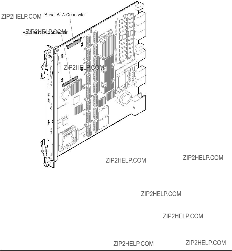
The blade allows to install one 2.5" hard disk which may be connected to either an on???board parallel or serial Advanced Technology Attachment (ATA) interface connector. The hard disk can be mounted directly on the blade without the need for an additional wire.aaa
Figure 5: Location of On???Board Hard Disk
The serial ATA interface supports up to 150 MByte/s data transfer rate and the parallel ATA supports all PIO and DMA modes up to Ultra ATA100. Hard disks which are connected to the parallel ATA interface act as master.a
Two hard disk accessory kits are available for the blade. One is called ACC/ATCA???715/HDD and contains a parallel ATA hard disk drive. The second is called ACC/ATCA???715/HDD???SATA and contains a serial ATA hard disk drive.a
Installing a Hard Disk

1.Position hard disk above blade so that the blade???s parallel ATA or serial ATA or SATA connector faces the hard disk???s interface connector
2.Connect hard disk with blade???s connectora
3.Turn blade to face its bottom side
4.Fasten four screws to blade???s bottom side
Removing a Hard Disk
1.Removing Hard Disk
2.Place blade on table with blade???s bottom side facing you
3.Remove four screws holding hard disk
4.Carefully remove hard disk from blades???s parallel ATA or SATA connector
5.Store hard disk and screws in a safe place in case you want to use the accessory kit components again
CompactFlash Disk
The blade provides a connector to install a CompactFlash card of type I and II.aaa
Figure 6: Location of CompactFlash Disk Connector
The CompactFlash card is operated in True IDE mode and is connected to the secondary IDE interface where it acts as IDE master.a
CompactFlash Installation
1. Open locking bow
2. Check that disk???s connectors face the CompactFlash socket

3. Plug CompactFlash into socket
4. Close locking bow over CompactFlash disk
Note:aThe locking bow must enclose the disk completely.a
Removal Procedure
1.Open locking bow
2.Take CompactFlash disk???s ends and pull CompactFlash disk carefully out of socket
3.Close locking bow again
CMC Debug Module
A CMC debug module is available as accessory kit for the blade. It is called ACC/ATCA???CMC???MODULE and provides two serial and one keyboard/mouse interface at its face plate. The CMC debug module is installed into PMC slot 4. For further details refer to theaACC/ATCA???CMC???MODULE Installation Guide.aa

Rear Transition Modules
At the time of writing this manual the following Rear Transition Modules (RTMs) was available for the blade: ACC/ARTM???717aa
It provides the following interfaces:a
STwo USB 2.0
STwo RS???232
SKeyboard/Mouse
SOne serial ATA
SFour RS???232 interfaces routed from PMC modules installed on the base blade
Note:a
SRefer to the RTM documentation for the RTM installation procedure
SCheck the documentation of the system where you operate the blade and the RTM for any restrictions that may apply to the blade or the RTM
SNo hot???swap is supported for the RTMs
The RTM furthermore incorporates an Intelligent Platform Management Interface Controller (IPMC) which enables you to monitor the RTM???s temperature and voltage sensors. For further information, refer to theaACC/ARTM???715/717/7105/7107: Control via IPMI Programmer???s Guideawhich can be downloaded from the former Force Computers S.M.A.R.T. server or the Motorola literature catalog.a

Blade Installation
The blade is fully compatible to the AdvancedTCA standard and is designed to be used in AdvancedTCA shelfs. Since the installation and removal procedures are different for powered and nonpowered shelfs, they are described in separate sections.aaaaa
Damage of Circuits
Electrostatic discharge and incorrect blade installation and removal can damage circuits or shorten their life.
Before touching the blade or electronic components, make sure that you are working in an ESD???safe environment.
Installation into Powered Shelves
Installation Procedure
1.Ensure that the top and bottom ejector handles are in the outward positionaa
2.Insert blade into the shelf by placing the top and bottom edges of the blade in the card guides of the shelf. Ensure that the guiding module of shelf and blade are aligned properly.a
3.Carefully slide the blade into the shelf until you feel resistance.a
If an RTM is already installed in the same slot, be careful not to bend any pins of the P30 to P32 backplane connectors.a
4.Hook the lower and the upper handle into the shelf rail recesses
5.Fully insert the blade and lock it to the shelf by pressing the two components of the lower and the upper handles together and turning the handles towards the face plate
As soon as the blade is connected to the backplane power pins, the blue LED is illuminated.a
When the blade is completely installed, the blue LED starts to blink. This indicates that the blade announces its presence to the shelf management controller.
Note:aIf an ARTM is connected to the front blade, make sure that the handles ofabotha the ARTM and the front blade are closed in order to power up the blade???s payload.
6.Wait until the blue LED is switched OFFa
The switched off blue LED indicates that the blade???s payload has been powered up and that the blade is active.a

7.Tighten the face plate screws which secure the blade to the shelfa
8.Connect cables to the face plate, if applicable
Removal Procedure
1.Remove face plate cables, if applicableaa
2.Unfasten the screws of face plate until the blade is detached from shelf
3.Open the lower and the upper handle by pressing the two handle components together and turning the handles outwarda
The blue LED blinks indicating that the blade power???down process is on???going.a
4.Wait until the blue LED is illuminated permanently
Note: if the LED continues to blink, a possible reason may be that upper layer software rejects the blade extraction request.a
Data loss
Removing the blade with the blue LED still blinking causes data loss.
Wait until the blue LED is permanently illuminated, before removing the blade.
5. Remove the blade from the shelf
Installation in Nonpowered Shelves
Installation Procedure
1.Power down the shelfaa
2.Ensure that the top and botton ejector handles are in the outward position
3.Insert blade into the shelf by placing the top and bottom edges of the blade in the card guides of the shelf. Ensure that the guiding module of shelf and blade are aligned properly.a
4.Slide the blade into the shelf until you feel resistance
If an RTM is already installed in the same slot, be careful not to bend any pins of the P30 to P32 backplane connectors.a
5.Hook the lower and upper handle into the shelf rail recessed
6.Fully insert the blade and lock it to the shelf by pressing the two components of the lower and upper handles together and turning the handles towards the face plate

7.Tighten the face plate screws which secure the blade to the shelf.a
8.Connect cables to the face plate, if applicable
Removal Procedure
1.Remove face plate cables, if applicableaa
2.Unfasten the screws of the face plate until the blade is detached from the shelf
3.Open the lower and the upper handle by pressing the two handle components together and turning the handles outward
4.Remove the blade from the shelf
Cable Accessory Kits
At the time of writing this manual the following cable accessory kits are available:aa
SACC/CABLE/PMC/RJ???45
SACC/CABLE/RJ45/DSUB
SACC/CABLE/USB
Note:aCheck with your local Motorola representative for the availability of further accessory kits.a
ACC/CABLE/PMC/RJ???45
The ACC/CABLE/PMC/RJ45 is an accessory kit compiled for the ACC/ARTM???717 rear transition module. It contains a splitter cable which allows to access the serial interfaces of PPMC???280 modules installed on the front blade via the ARTM???717 face plate.
ACC/CABLE/RJ45/DSUB
The ACC/CABLE/RJ45/DSUB/5E is an accessory kit containing a shielded cable of 2m length and an RJ???45/DSUB adapter plug. The cable provides Null???modem functionality which enables you to connect a laptop to the serial interface of the blade. The cable can be connected to either an installed CMC module or RTM.
ACC/CABLE/USB
The ACC/CABLE/USB/5E is an USB adapter cable of 200 mm length which converts the mini USB face plate connectors to USB A female.

3
Controls, Indicators, and Connectors

Face Plate
The following figure shows the connectors, keys and LEDs available on the face plate.a
P
M
C 1
OOS
OK
ACT
HDD
U
S
B
1P
M
C 2
U
S
B 2
P
M
C 3
R
E 
S
E
T
H/S
P
M
C 4
Figure 7: Face Plate
LEDs
The following figure shows all LEDs available at the face plate.aaa

OOS
OK
ACT
HDD
H/S
Figure 8: Location of Face Plate LEDs
The meaning of these LEDs is described in the following table.a
Table 7: Face Plate LEDs
Keys
The blade provides one face plate reset key.a
Reset
Key
P
M
C 3
R
E
S
E
T
Figure 9: Location of Reset Key
On pressing it, a hard reset is triggered and all attached on???board devices are reset.
Note:aThe IPMC is not reset via this key.a
Connectors
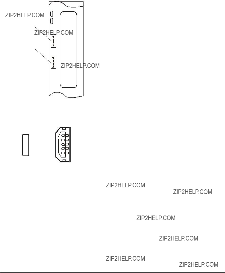
The blade provides two mini USB 2.0 connectors of type AB at its face plate. They correspond to the USB interfaces 1 and 2. An adapter cable accessory kit called ACC/CABLE/USB is available for the blade. It converts the mini USB male face plate connectors to USB female connectors.aaa
USB 1
USB 2
ACT
HDD
U
S
B
1P
M
C 2
U
S
B 2
Figure 10: Location of USB Connectors
Their pinout is given below.a
Figure 11: Face Plate USB Connector Pinout

On???Board Connectors
The blade provides the following on???board connectors:
SCompactFlash
SPMC
SParallel ATAa
SSerial ATA
SCMC
SATCA backplane connectors
Note:aThe blade may provide further on???board connectors. These are used for debug purposes only and are therefore not documented in this guide.a
CompactFlash
The CompactFlash connector is standard and is therefore not further described in this guide.a
PMC
The blade provides the four PMC sites PMC#1 to PMC#4. For each PMC site the four PMC connectors Pn1 to Pn4 are provided. See the following figure.aaa

Figure 12: Location of PMC Connectors Pn1 to Pn4
The connectors Pn1 to Pn3 implement the PMC pinouts as specified by the IEEE P1386.1 standard. Therefore they are not documented in this guide. The connector Pn4 contains PMC I/O signals and is described in the following.a
Pn4 carries the following types of signals:
SPower signals (GND)
SClock signals (CLK_*, NETREF))
SSignals routed to on???board Ethernet switch (ETH*_)
SSignals routed to RTM (PMC_IO_*)
Part of the signals that are routed to the on???board switch and RTM (with the exception of PMC_IO_25, 26, 28, 29, 30 and 31) are grouped into length???matched differential pairs of 100 ??? impedance.a

On the PMC sites 1 and 4, two Ethernet ports (signals named ETH*_) are routed to the on???board switch. On the PMC sites 2 and 3, only one port is routed to the on???board switch. The following two figures show the connector pinouts.aaa
Diff. Pair
Diff. Pair
Diff. Pair
Diff. Pair
Diff. Pair
Diff. Pair
Diff. Pair
Diff. Pair
Diff. Pair
Diff. Pair
Diff. Pair
Diff. Pair
11GND
{13 ETHB_DA+
15ETHB_DA???
17GND
{19 ETHB_DB+
21ETHB_DB???
23NETREF
25PMC_IO_25
27n.c.
29PMC_IO_29
31CLK8_B or PMC_IO_31
{33 PMC_IO_33
35PMC_IO_35
{37 PMC_IO_37
39PMC_IO_39
{41 PMC_IO_41
43PMC_IO_43
{45 PMC_IO_45
47PMC_IO_47
{49 PMC_IO_49
51PMC_IO_51
{53 PMC_IO_53
55PMC_IO_55
{57 PMC_IO_57
59PMC_IO_59
{61 PMC_IO_61
63PMC_IO_63
n.c.
n.c.
n.c.
n.c.
n.c.
GND ETHB_DC+ ETHB_DC???
GND ETHB_DD+ ETHB_DD??? n.c. PMC_IO_26 PMC_IO_28
CLK8_A or PMC_IO_30 n.c.
PMC_IO_34
PMC_IO_36
PMC_IO_38
PMC_IO_40
PMC_IO_42
PMC_IO_44
PMC_IO_46
PMC_IO_48 n.c. PMC_IO_52 PMC_IO_54 n.c. PMC_IO_58 PMC_IO_60 PMC_IO_62 PMC_IO_64
Figure 13: PMC Sites 1 and 4 ??? Pn4 Connector Pinout

Diff. Pair
Diff. Pair
Diff. Pair
Diff. Pair
Diff. Pair
Diff. Pair
Diff. Pair
Diff. Pair
Diff. Pair
Diff. Pair
Diff. Pair
Diff. Pair
{1 ETHA_DA+
3 ETHA_DA???
5 GND
{7 ETHA_DB+
9 ETHA_DB???
11GND
{13 ETHB_DA+
15ETHB_DA???
17GND
{19 ETHB_DB+
21ETHB_DB???
23NETREF
25PMC_IO_25
27n.c.
29PMC_IO_29
31CLK8_B or PMC_IO_31
{33 PMC_IO_33
35PMC_IO_35
{37 PMC_IO_37
39PMC_IO_39
{41 PMC_IO_41
43PMC_IO_43
{45 PMC_IO_45
47PMC_IO_47
{49 PMC_IO_49
51PMC_IO_51
{53 PMC_IO_53
55PMC_IO_55
{57 PMC_IO_57
59PMC_IO_59
{61 PMC_IO_61
63PMC_IO_63
ETHA_DC+
ETHA_DC???
GND ETHA_DD+ ETHA_DD???
GND ETHB_DC+ ETHB_DC???
GND ETHB_DD+ ETHB_DD??? n.c. PMC_IO_26 PMC_IO_28
CLK8_A or PMC_IO_30 n.c.
PMC_IO_34
PMC_IO_36
PMC_IO_38
PMC_IO_40
PMC_IO_42
PMC_IO_44
PMC_IO_46
PMC_IO_48 n.c. PMC_IO_52 PMC_IO_54 n.c. PMC_IO_58 PMC_IO_60 PMC_IO_62 PMC_IO_64
Figure 14: PMC Sites 2 and 3 ??? Pn4 Connector Pinout
Note:a
SThe signals available at pins 30 and 31 depend on the settings of the on???board switches SW7???1 to SW7???4. Seeasection "Switch Settings" on pagea42a for further details.a
SBy default, the PMC I/O Ethernet signals (ETH_xxx) are routed to the on???board switch via magnetics. As an assembly option the magnetics can be by???passed and the Ethernet signals can be accessed via an installed PMC uplink module from Motorola. Consult your local Motorola representative for details.a
SBy default the signals at pins 61 to 64 are routed the zone 3 connectors where they are available as PMC I/O signals. As an assembly option these signals can be routed to the on???board Ethernet switch as further 100BaseTX interface. Consult your local Motorola representative for details.a
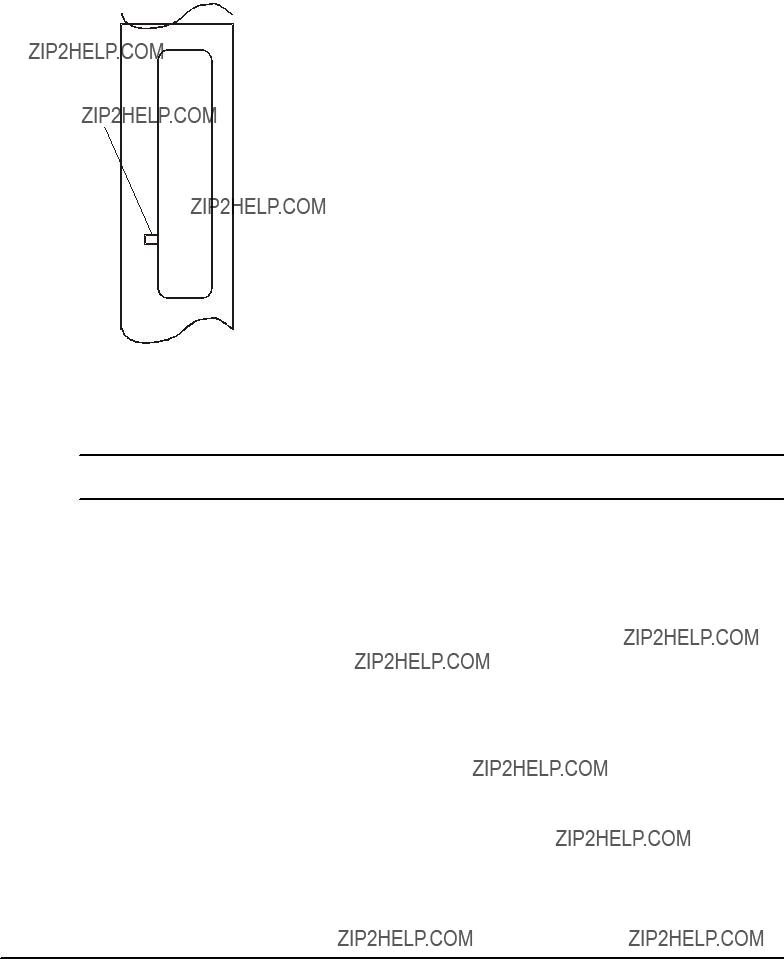
Parallel ATA Connector
The blade provides one parallel Advanced Technology Attachment (ATA) connector which allows to connect a 2.5" hard disk to the blade. The location of this connector is shown in the following figure.aaa
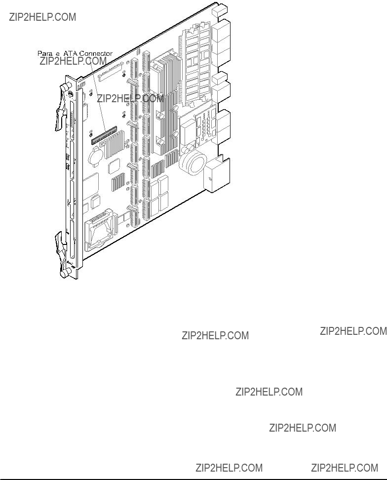
Figure 15: Location of Parallel ATA Connector
The pinout of the connector is as follows.a

Figure 16: Parallel ATA Connector Pinout
Serial ATA Connector
The blade provides one Serial Advanced Technology Attachment (SATA) connector which allows to connect a hard disk to the blade. The location of the SATA connector is shown in the following figure.aaa

Figure 17: Location of Serial ATA Connector
The pinout of the SATA connector is given in the following figure.a
CMC Module Connector
The blade provides one CMC connector which allows to connect a CMC debug module to the blade. A CMC debug module is available as accessory kit for the blade. The CMC module uses the same mounting holes as PMC slot #4.a
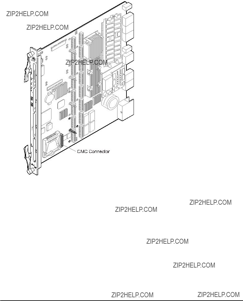
Figure 18: Location of CMC Connector
The pinout of the CMC connector is given in the following figure.a

2
4
6
8
10
12
14
16
18
20
22
24
26
28
30
32
34
36
38
40
42
44
46
48
50
52
54
56
58
60
62
64
For further information about the CMC module refer to theaACC/ATCA???CMC???MODULE Installation Guide.aa
AdvancedTCA Backplane Connectors
The AdvancedTCA backplane connectors reside in the three zones 1 to 3 as specified by the AdvancedTCA standard and are called P10, P20, P22, P23, P30, P31, and P32. The location of these connectors is shown in the following figure.aaa

The pinouts of all these connectors are given in this section.a
The connector residing in zone 1 is called P10 and carries the following signals:
SPower feed for the blade (ABP_VM48_x_CON and ABP_RTN_A_CON)
SPower enable (ABP_ENABLE_x)
SIPMB bus signals (APMB_P10_IPMB0_x_yyy)
SGeographic address signals (ABP_P10_HAx)
SGround signals (ABP_P10_SHELF_GND and GND)
SReserved signals

18n.c.
19n.c.
20n.c.
21n.c.
22n.c.
23n.c.
24n.c.
25ABP_P10_SHELF_GND
26GND
27ABP_ENABLE_B
28ABP_RTN_A_CON
29ABP_RTN_B_CON
30n.c.
31n.c.
32ABP_ENABLE_A
33ABP_VM48_A_CON
34ABP_VM48_B_CON
Figure 19: P10 Backplane Connector Pinout
Zone 2 contains the three connectors P20, P22 and P23. They carry the following types of signals:
STelecom clock signals (CLKx_)
SBase interface signals (BASE_)
SFabric channel interfaces (FAB_)
Some of the pins provided by P20, P21 and P23 are defined as optional in the AdvancedTCA specification and are unused on the blade. If the AdvancedTCA specification defines these signals as input signals, they are terminated on the blade and marked as "TERM_" in the following pinouts. In all other cases the pins are unconnected and consequently marked as "n.c.".a
The pinouts of P20, P21 and P23 are as follows.a
Figure 20: P20 Backplane Connector Pinout ??? Rows A to D
Figure 22: P22 Backplane Connector Pinout ??? Rows A to D

Figure 23: P22 Backplane Connector Pinout ??? Rows E to H
a
b
1n.c.
2FAB2_TX+
3n.c.
4FAB1_TX+
5BASE_DA1+
6BASE_DA2+
7n.c.
8n.c.
9n.c.
10 n.c.
n.c.
FAB2_TX???
n.c.
FAB1_TX+ BASE_DA1??? BASE_DA2???
n.c.
n.c.
n.c.
n.c.


 TERM_RX2_2+


 FAB2_RX+


 TERM_RX1_2+


 FAB1_RX+


 BASE_DB1+


 BASE_DB2+


 n.c.
n.c. 


 n.c.
n.c.


 n.c.
n.c.
Figure 24: P23 Backplane Connector Pinout ??? Rows A to D
Figure 25: P23 Backplane Connector Pinout ??? Rows E to H

Zone 3 contains the three connectors P30 to P32. They are used to connect an RTM to the blade and carry the following signals
SSerial (RS232_x_yyyy)
SSerial ATA (SATAx_yyy)
SUSB (USBxy)
SKeyboard/Mouse (KBD_xxx, MS_xxx)
SIPMI (IPMB1_xxx, ISMB_xxx))
SPower (VP12_RTM, V3P3_RTM)
SPMC user I/O (PMCx_IO_yy)
SGeneral control signals (BD_PRESENTx, RTM_PRSNT_N, RTM_RST_KEY*, RTM_RST*)
a
1R232_2_RXD
2RS232_2_DCD???
3RTM_GPO
4USB0+
5n.c.
6n.c.
7SATA0_TX+
8n.c.
9IPMB1_SCL
10 VP12_RTM
Figure 26: P30 Backplane Connector Pinout ??? Rows A to D
Figure 27: P30 Backplane Connector Pinout ??? Rows E to H

Figure 28: P31 Backplane Connector Pinout ??? Rows A to D
Figure 29: P31 Backplane Connector Pinout ??? Rows E to H
Figure 30: P32 Backplane Connector Pinout ??? Rows A to D
Figure 31: P32 Backplane Connector Pinout ??? Rows E to H
4
BIOS

Introduction
BIOS (Basic Input Output System) provides an interface between the operating system and the hardware of the blade. It is used for hardware configuration. Before loading the operating system, BIOS performs basic hardware tests and prepares the blade for the initial boot???up procedure.
During blade production, identical BIOS images are programmed into the blade???s boot and user flash. By default the blade boots from the boot flash. It is possible to select between boot and user flash as device to boot from. This is done via a OEM IPMI command. For further details refer to theaPENT/ATCA???715/717/7105/7107: Control via IPMI Programmer???s Guidea which can be downloaded from the Motorola literature catalog. The presence of two redundant flash devices also allows for updating the BIOS image without affecting running processes.aaa
The BIOS used on the blade is based on the Phoenix 4.0 Release 6.0 BIOS with several Motorola extensions integrated. Its main functions are:
SHardware set???up utility for setting configuration data
SMultiboot for a flexible boot order
SSerial console redirection for remote blade configuration
SSoftware upgrade utility
Note:aThe BIOS contains on???line documentation which provides detailed description of all BIOS functions. Therefore the description in this manual is restricted to the main BIOS functions.a
The BIOS set???up program is required to configure the hardware of the blade. This configuration is necessary for operating the blade and connected peripherals. It is stored in the battery backed???up CMOS memory as well as in the blade???s boot flash.a
Whenever you are not sure about configuration settings, restore the default values. They are provided in case a value has been changed and you wish to reset settings. To restore the default values, press <F9> in setup.
Note:a
SLoading the BIOS default values will affect all set???up items and will reset options previously altered.a
SIf you set the default values, the displayed default values are not yet stored to be effective for the next boot. They are just loaded to be displayed. However, they become effective if the BIOS setup is exited after changes have been saved.

The BIOS complies to the following specifications:
SPlug and Play BIOS Specification 1.0A
SPCI BIOS Specification 2.1
SSMBIOS Specification 2.3
SBIOS Boot Specification 1.01
SPXE 2.0
Serial Console Redirection
The firmware of the blade provides a serial console redirection feature. This allows remote blade configuration by connecting a terminal to the blade via a serial communication link.a
The terminal can be connected to display VGA text information. Terminal keyboard input is redirected and treated as a normal PC keyboard input. The serial console redirection feature can be configured via setup utility.
Note:aIf serial console redirection is enabled the terminal represents an option and is not necessarily required for boot???up procedure.a
Requirements
For serial console redirection, the following is required:
STerminal which supports a VT100 or ANSI modea
SNULL???modem cable
Terminal emulation programs such as TeraTermPro can be used. In order to use TeraTermPro via the function keys, the keyboard configuration file of TeraTermPro has to be modified as follows:
Table 8: Key Codes for Terminal Emulation Program
Default Configuration
By default, the blade can be accessed via the serial interface COM1. This interface is, by default, accessible via an installed RTM through an RJ???45 connector. If no RTM is present or you wish to access COM1 from the blade???s face plate, COM1 can alternatively be made accessible at an installed CMC module. Whether COM1 is available via RTM or CMC module depends on the setting of the on???board switch SW3???4 which enables/disables COM port swapping. The following table provides details.aaa

Note:a
SThe COM port routing described above is only applicable to BIOS versions w 2.0.0. Earlier BIOS versions used a different routing. For details refer to theaPENT/ATCA???715/717/7105/7107 BIOS Information Sheeta which can be downloaded from the Motorola literature catalog web site.
SCOM port swapping can also be enabled via an IPMI System Boot Options command. COM port swapping is enabled if either the on???board switch 3???4, the IPMI System Boot Options command or both enable it.a
A NULL???Modem cable is available as accessory kit for the blade. It converts the RJ???45 connector to a standard DSUB connector which can be connected to a remote terminal. The following communication parameters are used by default:
SBaud rate: 9600
SNo handshake
SPC ANSI
S8 data bits
SNo parity
S1 stop bit
All configuration parameters listed above can be modified via the BIOS.a
Connecting to the Blade
In order to connect to the blade using the serial console redirect feature, proceed as follows:.
Procedure
1.Configure terminal to communicate using the same parameters as in BIOS setup
2.Connect terminal to NULL???modem cable
3.Connect NULL???modem cable to COM port you have selected in BIOS setup
4.Start up blade
BIOS Crisis Recovery Mode
Immediately after a reset or power???up a routine in the boot flash boot block is invoked which checks whether a valid BIOS image is available. If no valid image is found and consequently the blade is unable to boot, the blade enters into BIOS crisis recovery mode. In this mode a routine tries to load a BIOS crisis recovery image from a disk drive connected to the blade??? s USB interface. The BIOS crisis recovery image is basically a mini DOS with minimum functionality which replaces the corrupted image.a
A valid BIOS crisis recovery image can be downloaded from the former Force Computers SMART server or the Motorola website as part of the BIOS upgrade kit which which is available for this blade. The image is accompanied by readme files which describe how to create the BIOS upgrade/recovery disk and how to to replace a corrupted BIOS with the BIOS crisis recovery image.a
If the blade has enterred BIOS crisis recovery mode,the face plate LED "HDD" is lit ed. After the BIOS recovery image has been successfully flashed, the LED is lit green.a
Note:aFlashing the BIOS crisis recovery image may take up to two minutes. In order to avoid blade damage, it is absolutely important not to interrupt the flashing process. Therefore wait until the LED is lit green again, which indicates a successful flashing.a

Changing Configuration Settings
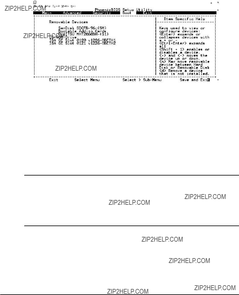
When the system is turned on or rebooted, the presence and functionality of the system components is tested by POST (Power???On Self???Test).a
Press <F2> when requested. The main menu appears. It looks similar to the menu shown in the following figure. Note that the layout may slightly vary with new BIOS versions.a
Figure 32: Main Menu
Note:a
SMake sure that BIOS is properly configured prior to installing the operating system and its drivers.
SIf you save changes in setup, the next time the blade boots BIOS will configure the system according to the setup selections stored. If those values cause the system boot to fail, reboot and enter setup to get the default values or to change the selections that caused the failure. If the boot fails or is interrupted three times in a row, the default values are then loaded automatically.
In order to navigate in setup, use the arrow keys on the keyblade to highlight items on the menu. All other navigation possibilities are shown at the bottom of the menu.
Additionally, an item???specific help is displayed on the right side of the menu window.

Selecting The Boot Device
There are two possibilities to determine the device from which BIOS attempts to boot:
SVia setup to select a permanent order of boot devices
SVia boot selection menu to select any device for the next boot???up procedure only
Via Setup
1.In the menu line, select [Boot]
A menu similar to the one shown in the following figure appears. Note that the layout may vary slightly with new BIOS versions.a
2.Select [Boot Device Priority]
A menu similar to the one shown in the following figure appears. Note that the layout may vary slightly with new BIOS versions.a
3.Select the order of the devices from which BIOS attempts to boot the operating system
If BIOS is not successful at booting from one device, it tries to boot from the next device on the list.
If there is more than one device of the same type, e.g. several hard disks, the displayed entry represents the first of these devices as specified in the boot configuration via setup.
The same options determine the order in which POST installs the devices and the operating system assigns device letters. BIOS supports up to two floppy devices to which the operating system may assign, e.g. drive letters A: and B:. The drives C:, D:, E: etc. are reserved for hard???disk drives.
Note:aThere is not always an exact correspondence between the order specified in setup and the letters assigned by the operating system. Many devices, such as legacy option ROMs, support more than one device that can be assigned to several letters. If the CD???ROM drive should have a letter coming before the one assigned to the hard drive, move it in front of the hard drive. The group of bootable add???in cards refers to devices with non???multiboot???compliant BIOS option ROM from which you can boot the operating system.a
Via Boot Selection Menu
To enter the boot menu, press <ESC> during POST. The menu that appears looks similar to the one shown in the following figure. Note that the layout may vary slightly with new BIOS versions.a

Figure 33: Boot Menu
Continue with one of the following options:
a)Override existing boot sequence by selecting another boot device from the boot order list or
b)Select [Enter Setup] to enter setup utility or
c)Press <Esc> to return to POST screen and continue with previous boot sequence
Note:aIf the selected device does not load the operating system, BIOS reverts to the previous boot sequence.
Restoring BIOS Default Settings
The blade provides an on???board configuration switch that allows to clear the blade???s CMOS and thus to restore the BIOS default settings. In order to restore the BIOS default settings using this switch, you have to proceed as follows.aa
Procedure
1.Remove the blade from the system
Seeasection "Installation into Powered Shelves" on pagea54a for the exact procedure
2.Set the on???board switch SW2???3 to ON
Seeasection "Switch Settings" on pagea42a for the exact location of SW2???3
3.Install and power up the blade
Seeasection "Installation into Powered Shelves" on pagea54a for the exact procedure.a Note that the blade will not boot, because the "Clear CMOS RAM" switch SW2???3 is set to ON.a
4.Remove the blade from the system again
Seeasection "Installation into Powered Shelves" on pagea54a for the exact procedure
5.Set switch SW2???3 to OFF
Now the BIOS default settings are restored.a

Updating BIOS
For the blade a BIOS upgrade kit is offered. It is available via the former Force Computers S.M.A.R.T. web site or the Motorola web site.aaa
Note:aWhen upgrading the BIOS, all BIOS settings are reset to their default state.a

BIOS Messages
If your system fails after you made changes in the setup menus, you may be able to correct the problem by entering setup and restoring the original values.a
None
Check that drive is defined with proper disk type in setup, that disk drive is attached correctly and that controller is enabled.
None
Check if memory modules are installed correctly. Otherwise contact your local sales representative or FAE for further support.
None
Check if memory modules are installed correctly. Otherwise contact your local sales representative or FAE for further support.

Enter setup and check if fixed disk and drive A: are properly identified.
Check for correct memory module types.
Press <F1> to start boot process or <F2> to enter setup and change any settings.
Run setup to restore original configuration. This error is cleared the next time the system is booted.
May require blade repair
Run ISA or EISA Configuration Utility to resolve resource conflict.
Contact your local sales representative or FAE for further support.
None

Check for correct memory modules. Otherwise contact your local sales representative or FAE for further support.
None

BIOS Post Codes
The following table lists BIOS post codes applicable to the used Phoenix 4.0 Release 6.0 BIOS. The BIOS POST codes are stored in the blade???s Port 80 register and can also be obtained by reading an on???board IPMI sensor. For details refer to theaPENT/ATCA*715/717/7105/7107: Control via IPMI Programmer???s Guide which can be downloaded from the Motorola literature catalog.aaa
Table 9: Standard BIOS Post Codes
10initialize power management
11Load alternate registers with initial POST values
12Restore CPU control word during warm boot
13Initialize PCI bus mastering devices
14Initialize keyboard controller
16BIOS ROM checksum
17Initialize cache before memory autosize
188254 programmable interrupt timer initialization

28Autosize DRAM
29Initialize POST memory manager
32Test CPU bus clock frequency
33Initialize Phoenix Dispatch Manager
41Initialize extended memory for RomPilot
42Initialize interrupt vectors
45POST device initialization
46Check ROM copyright notice
47Initialize I20 support
48Check video configuration against CMOS
49Initialize PCI bus and devices
50Display CPU type and speed
51Initialize EISA board

54Set key click if enabled
55Enable USB devices
58Test for unexpected interrupts
59Initialize POST display service
66Configure advanced cache registers
67Initialize Multi Processor APIC
68Enable external and CPU caches
69Setup system management mode (SMM) area
80Disable onboard super I/O ports and IRQ???s
81Late POST device initialization
82Detect and install external RS232 ports
83Configure non???MCD IDE controllers
84Detect and install external parallel ports

Post Code Description
85Initialize PC compatible PnP ISA devices
86Reinitialize onboard I/O ports
87Configure motherboard configurable devices (optional)
88Initialize BIOS data area
89Enable non???maskable interrupts (NMI???s)
90Initialize hard disk controllers
91Initialize local bus hard disk controllers
92Jump to UserPatch2
93Build MPTABLE for multi processor boards
95Install CD ROM for boot
96Clear huge ES segment register
97Fixup multi processor table
98Search for option ROM???s
99Check for SMART drive (optional)


5
Devices??? Features and Data Paths


Block Diagram
Figure 34: Base Board Block Diagram

CPU
The used Central Processing Unit (CPU) is a Pentium M processor. The CPU provides 32 kBytes of on???die data and instruction cache as well as two MByte L2 cache.aaa
An on???die temperature sensor measures the CPU temperature. It is connected to the blade???s Intelligent Peripheral Management Controller (IPMC). This way software can monitor the CPU temperature via IPMI.aaa

Host Bridge
The used host bridge is an Intel E7501 Memory Controller Hub (MCH) device. It is part of the Intel Plumas chipset and provides bus control signals, address and data paths for transfers between the CPU front side bus, main memory and the four hub interfaces provided by the host bridge.aaa
Host Interface
The host interface supports a 64???bit wide data bus and a 32???bit wide address bus. The data bus is quadpumped and runs at 100 MHz, resulting in a total bandwidth of 3.2 GB/s. The memory bus is double pumped and supports an address range of up to 4 GByte. Its bandwidth is 200 Mb/s per data line resulting in a total bandwidth of 128 x 200MB/S = 3.2GB/s.a
Memory Interface
The memory interface is a 144???bit wide SDRAM interface supporting 64, 128, 256 and 512 MBit DDR SDRAM technology. The bus speed is 100 MHz running synchronously to the front side bus. Additionally ECC is supported.a
Although theoretically up to 16 GByte are supported by the memory interface, the actual maximum memory size is limited to 4 GByte due to the CPU???s 32???bit address bus.a
Hub Interfaces
The Host Bridge provides the four hub interfaces A, B, C and D.a
Hub interface A is quad pumped, 8???bit wide and runs at 66 MHz. It is connected to the South Bridge and provides a maximum data transfer rate of 266MByte/s. Parity protection is provided for hub interface A. Any parity errors are detected by the host bridge and reported to the South Bridge, which in turn generates an NMI.a
The hub interfaces B, C and D are octal pumped, 16???bit wide and run at 66 MHz. The maximum data transfer rate provided by each hub interface is 1.066 GByte/s.a
ECC protection is provided for hub interfaces B, C and D. Any ECC errors are detected by the host bridge and reported to the South Bridge, which in turn generates an NMI.a

South Bridge
The used South Bridge is an Intel 6300ESB I/O controller hub device. It provides the interface between the Host Bridge and the legacy I/O. Integrated into the South Bridge are:aa
STwo 8237 DMA controllers
SOne 8254 counter timer
SInterrupt controller
SReal???time clock
SWatchdog
The interfaces provided by the South Bridge include:a
SHub interface 1.5
SPCI 2.2 interface
SPCI???X 1.0 interface
STwo parallel ATA interfaces
STwo serial ATA interfaces
STwo serial RS???232 interfaces
SFour USB interfaces
SLPC interface
SSMBus interface
Interrupt Controller
The interrupt controller residing in the South Bridge is 8259A???compliant and runs in PIC mode.a
The interrupts of the four PMC slots are merged and are routed through an FPGA to the interrupt controller where they are mapped to ISA compatible interrupts.a
The interrupt controller is also able to generate CPU Non???Maskable Interrupts (NMIs). Possible sources of NMIs are:aa
SMemory ECC and parity errors

SHub interface ECC and parity errors
SPCI bus parity errors
Real???Time Clock
The Real???Time Clock (RTC) resides inside the South Bridge and is sourced by an external 32.768 crystal providing a frequency tolerance of 20 ppm. The RTC provides 242 bytes backed???up CMOS RAM and is fully compliant to:aa
SDS1287
SMC14618
SY2K
SPC87911
Watchdog
The Southbridge incorporates a two???stage watchdog timer. For details refer to the Intel 6300ESB I/O controller documentation. On expiry, the watchdog is able to issue a blade reset.a
PCI???X Interface
The PCI???X interface is 64???bit wide and runs at 66 MHz. It is compliant to the PCI???X 1.0 specification. On the board 3.3V signalling level is used and an 82546EB/GB dual Ethernet controller is connected to the PCI???X interface.a
Parallel ATA Interfaces
The South Bridge provides two separate parallel Advanced Technology Attachment (ATA) interfaces: one primary and one secondary parallel ATA interface. Both interfaces support all Programmed I/O (PIO) modes as well as all Direct Memory Access (DMA) modes up to Ultra ATA/100. The combined parallel and serial ATA interface traffic is indicated by a face plate LED.a
Primary Parallel ATA Interface
The primary parallel ATA interface is connected to an on???board 2.5" hard disk which can be mounted on the blade. The hard disk operates as IDE master.a

Secondary Parallel ATA Interface
The secondary parallel ATA interface is connected to an on???board CompactFlash connector which supports CompactFlash cards of type I and II. An inserted card runs in true IDE mode and is master on the secondary parallel ATA interface.a
USB Interfaces
The South Bridge provides four USB interfaces. Two are routed to the blade???s face plate and two to the rear transition module. All interfaces are compliant to the USB 2.0 standard.a
PCI Interface
The South Bridge provides a 32???bit/33 MHz PCI interface that is compliant to the PCI 2.2 specification. Up to four external PCIbus master devices are supported and a 3.3V signaling level is used.
Serial ATA Interfaces
The South Bridge provides two Serial Advanced Technology Attachment (SATA) interfaces which are compliant to the SATA 1.0 specification and support a data transfer rate of up to 1.5GByte/s. One interface is routed to the Zone 3 connector and is accessable via an installed RTM. One interface is routed to an on???board SATA connector to which a SATA hard disk can be connected.a
Serial RS232 Interfaces
The South Bridge provides two serial full???duplex RS232 interfaces. Supported baud rates are: 600, 1200, 2400, 4800, 9600, 19200, 38400 and 115200 kb/s. Both serial interfaces are +/??? 15 KV ESD protected.
Both interfaces correspond to the blade???s serial interface ports 1 and 3. Serial interface port 1 is routed via a zone 3 connector to an installed RTM. Serial interface port 3 is accessible via an installed CMC module. The BIOS maps the serial interfaces ports to the desired I/O addresses (COM ports) and interrupts.aaaaa
LPC Interface
The South Bridge provides a 4???bit wide Low Pin Count (LPC) interface running at 33 MHz. It has the following devices attached to it:
SSuper I/O
SBoot flash
SUser flash
SGlue Logic FPGA
SMBus Interface
The following table lists all devices which are connected to the South Bridge via its SMBus interface:aaaa

Super I/O
The used Super I/O is a Standard Microsystems Corporation LPC47S422 device. It provides the following interfaces:aa
STwo serial interfaces
SFloppy disk interface
SKeyboard/Mouse interface
SParallel interface
Serial Interfaces
The Super I/O device provides two serial full???duplex RS232 interfaces. Supported baud rates are: 600, 1200, 2400, 4800, 9600, 19200, 38400 and 115200 kb/s. Both serial interfaces are +/??? 15 KV ESD protected.
Both interfaces correspond to the blade???s serial interface ports 2 and 4. Serial interface port 2 is routed via a zone 3 connector to an installed RTM. Serial interface port 4 is accessible via an installed CMC module. The BIOS maps the serial interface ports to the desired I/O addresses (COM ports) and interrupts.aaaaa
Floppy Disk Interface
The floppy disk interface is unused on the blade.a
Keyboard/Mouse Controller
The Super I/O integrates an 8042H compatible keyboard/mouse controller. The corresponding interfaces are accessible via RTM and CMC debug module.a
Parallel Interface
The parallel interface is unused on this blade.

Flash Devices
The blade provides two redundant boot flash devices: one default boot flash and one backup boot flash. During blade production, both flashes are programmed with identical BIOS images. The presence of two redundant flash devices allows for remotely updating BIOS images from the operating level without interrupting running processes and without being affected by possibly corrupt BIOS images. The backup boot flash, furthermore, can be used to store customized images. Note that in this case the redundant BIOS feature is no longer available.a
Both flash devices are Intel???compatible firmware hubs that are connected to the LPC interface of the South Bridge. Each flash device has a unique four bit LPC device ID. Bit 1 to 3 of the device ID are fixed to 0. Bit 0 is controlled by a boot flash select signal provided by the IPMC in such a way that bit 0 of one flash is set to 0 while bit 0 of the other flash is set to 1 and vice versa. The following figure shows the implementation on hardware???level.a
Figure 35: Boot Flash LPC Device ID Control
The blade??? s CPU always boots from the boot flash with the LPC device ID 0. Thus the boot flash select signal of the IPMC allows to select the flash device that the CPU is to boot from.a
An IPMI Set System Boot Options command allows to control the boot flash select signal and thus select between the default and backup boot flash as device to boot from. For details refer to theaPENT/ATCA???715/717/7105/7107: Control via IPMI Programmer???s Guidea which can be downloaded from the former Force Computers S.M.A.R.T. server or the Motorola literature catalog.aaaaaaaa
By default, the data/instruction areas of the default and backup boot flash are writable. This is necessary because during booting the BIOS writes some configuration data back to

some reserved spaces in the data/instruction area. The boot block of default and backup boot flash are writeable per default, too. The on???board switches SW4???1, SW4???2 and SW4???4 allow to enable/disable the write???protection of both default and backup boot flash as well as the data/instruction area of the backup boot flash.a

FPGA
The FPGA implements the following functions:aaaaa
SLPC interface
SIPMC interface
SClock synchronization extensions
SReset controller
SInterrupt routing unit
SMiscellaneous glue logic
SEthernet switch interface
The FPGA loads its configuration stream from one of two EEPROMs which are connected to the FPGA. One EEPROM serves as default, the second as backup EEPROM. The IPMC controls which EEPROM the configuration stream is loaded from. After IPMC startup the FPGA loads its configuration stream from the default EEPROM. An IPMI System Boot Options command allows to select between default and backup EEPROM. For details about switching between default and backup FPGA refer to theaPENT/ATCA???715/717/7105/7107: Control via IPMI Programmer???s Guidea which can be downloaded from the Motorola literature site.aaa
LPC Interface
The LPC interface is compliant to the Intel LPC specification 1.1 and connects the FPGA to the South Bridge.a
IPMC Interface
The FPGA is connected to the on???board IPMC and implements the following IPMC related features:
STwo Block Transfer interfaces
SPort 80 register
SIPMC extensions
Block Transfer Interfaces
Two Block Transfer interfaces (BT) reside inside the FPGA. Each provides one control and status register, two 64???byte FIFOs and an interrupt mask register. Both BT interfaces are

compliant to the IPMI specification V1.5 Rev. 1.0 and share one Interrupt Source register. The first BT interface is used as the only System Interface and uses IPMI channel 0x0F. The second BT interface uses IPMI channel 0x06.aaa
Port 80 Register
The FPGA provides an 8???bit wide register to store POST codes. The register is located at I/O address 8016.. It is only readable for the IPMC and read???writeable for the host. The IPMC polls this register to monitor the boot up sequence of the board. The content of the port 80 register can also be obtained and read via IPMI.a
IPMC Extensions
The FPGA implements three registers which are only visible for the IPMC. These registers reflect the following:
SCPU core voltage identifier
SFrame signal on LPC bus
SSystem and parity errors on PCI buses
SEnabling/disabling of backplane signals used for electronic keying
SAlert signals
Clock Synchronization Extensions
The FPGA contains extensions which are related to the AdvancedTCA clock synchronization feature. These extensions include:
SRegisters accessible via host and IPMC for controlling and monitoring clock synchronization
SSPI interface for controlling DPLL device
SProgrammable clock dividera
For further details refer toasection "Clock Synchronization Interface" on pagea124a andasection "Clock Synchronization Interface Registers" on pagea144.
Reset Controller
The FPGA contains part of the blade???s reset logic. Furthermore it provides two registers which allow to determine the source of the last reset issued and to mask resets.a
Reset Types
Two different types of resets are possible: hard resets and soft resets.a

During a hard reset all internal registers, state machines and caches of the CPU are reset. Furthermore all on???board PCI devices as well as the host bridge are reset.a
During a soft reset the CPU is reset, with the exception of the internal caches and state machinesaaa
Reset Sources
The following table lists all possible reset sources and the corresponding reset types.aaa
Table 10: Reset Sources
Interrupt Routing Unit
The FPGA is used for fixed interrupt routing on the blade.a
All interrupts from PCI devices are routed via the FPGA to the South Bridge. All other interrupts are routed to the Super I/O device from where they are routed to the South Bridge.a
Miscellaneous Glue Logic
The miscellaneous glue logic includes:
SSerial interface
SReset mask and source register
SFlash control register
SPMC status register
SShut???down register

SLEDs
SVersion register
Serial Interface
The FPGA provides routing options of one of the two serial interfaces provided by the Southbridge. This feature is intended for Motorola???internal purposes and should be ignored. .a
Reset Mask and Source Register
The FPGA provides two registers which allow to obtain the last reset source and to mask resets. Seeasection "Reset Registers" on pagea139.a
Flash Control Register
The FPGA provides one register which allows to monitor the boot and user flash write???protection status as well as to control the write???protection of the boot flash boot block. Seeasection "Flash Control and Status Register" on pagea141
PMC Status Register
The FPGA provides one register which allows to monitor the status of the four PMC sites. Seeasection "PMC Status Register" on pagea143
Shut???Down Register
The FPGA provides one register which allows to control the blades??? FRU???EN signal. Seeasection "Shut Down Register" on pagea143
LEDs
The FPGA provides a register to control the HDD LED available at the face plate. This LED indicates the combined parallel and serial ATA activity or is operated in user LED mode. Seeasection "LED Control Register" on pagea142.a
Version Register
This register allows to obtain the current FPGA version. Seeasection "Version Register" on pagea147.a

Intelligent Platform Management Controller
The blade provides an Intelligent Platform Management Controller (IPMC) unit based an the 8???bit Atmel ATmega AVR microcontrollers. The IPMC is fully compliant to the IPMI V1.5 standard and provides the following interfaces:aaa
SIPMB0A and IPMB0B available via the backplane
SIPMB???L connected to rear transition modulea
SI2C interfaces connected to on???board PMCs slots and sensors
SAnalog???to???Digital Conversion (ADC)interfaces connected to on???board sensors
SDigital I/O interfaces connected to on???board sensors
One of the main tasks of the IPMC is to control the power up and power down of the blade. For this purpose the IPMC is connected to the on???board power supply module via control and status lines. Various on???board IPMI sensors provide detailed information on the current power status of the blade to any interested party connected to the IPMI network.a
The following figure gives an overview of the IPMI structure used on???board.aaa
Figure 36: IPMI Structure
For details about accessing the IPMC via IPMI commands as well as Sensor Data Records (SDRs) and Field Replacable Unit (FRU) information provided by the blade, refer to the "PENT/ATCA???715/717/7105/7107 Control via IPMI Programmer???s Guide" which can be downloaded from the Motorola literature catalog.a

Sensors
The blade provides various sensors which are accessible via IPMI. Some of these sensors measure on???board temperatures. Their names and locations are shown in the following figure.aaa
Memory Temp
CPU Board Temp (other side of PCB)
CPU Die Temp
12V DCDC Temp
Ambient Temp
Figure 37: IPMI Temperature Sensors
Other sensors available on???board include voltage sensors and sensors which provide particular status information. A summary of all sensors is given in the following table.a
Table 11: On???board Sensors Accessible via IPMI


For further details refer to the "PENT/ATCA???715/717/7105/7107 Control via IPMI Programmer???s Guide" which can be downloaded from the Motorola literature catalog.
I2C Addresses
The blade provides one IDROM which is attached to the IPMC via an I2C bus. The I2C address of the IDROM is 0xA0.a

Clock Synchronization Interface
AdvancedTCA systems provide a telecom clock synchronization interface which allows to synchronize elements within a telecommunication network. The telecom clock synchronization interface consists of three redundant clock buses (CLK1, CLK2 and CLK3) which are available at the system backplane. Each clock bus is implemented as a differential pair of MDS/LDS signals which connects to each system slot.aaa
In compliance with the AdvancedTCA PICMG 3.0 specification, CLK1 and CLK2 are used as system clocks and CLK3 is used as reference clock.a
The blade provides a clock synchronization building block which allows to synchronize the four on???board PMC modules to the system clock and to derive a reference clock. The main components of the clock synchronization building block as well as the main signal paths are shown in the following figure.aaa
The key component of the clock synchronization building block is the DPLL device ACS8525 from Semtech. Its main features include:
SSoftware programmable output clock synthesis (CLK_0, 1, 2, 3)

S8 kHz frame clock/pulse with programmable pulse width and polarity (SYNC_0,1,2,3))
SAutomatic hit???less switch???over if one system clock fails
SActivity monitor for system clocks
SPhase build???out for output clock phase continuity during switch???over
SMeets jitter requirements up to OC???3 line rates
SProgrammable reference clock divider
The DPLL is clocked by an external oscillator running at 12.8 MHz. Two clock buffers provide a separate clock and synchronization signal for each of the four on???board PMC sites. The FPGA contains extensions which are related to the clock synchronization building block. Some of these extensions include registers that are accessible via the host and which allow to control and monitor the functionality of the clock synchronization building block. For details refer toasection "Clock Synchronization Interface Registers" on pagea144.a

Power Supply Module
The blade is fed via two redundant ???48V inputs. Both are converted via a DC/DC converter to an intermediate voltage of +12V. This voltage, in turn, is converted via further DC/DC converters to on???board voltages which are used by the on???board devices. A ???48V/+3.3V DC/DC converter converts the ???48V input voltage to +3.3V which is used to feed the IPMC and power???up logic.
The blade???s power up and power down cycles are under full control of the IPMC. It controls both the ???48V/+12V DC/DC converter as well as power???up logic which controls the remaining on???board DC/DC converters. If the IPMC detects a failure on any of the local on???board voltages, it shuts off the entire blade power.aaa
The blade???s power supply structure is shown in the following figure.a
???48V_A
???48V_B
Return_A
Return_B
???48V_A
???48V_B
Return_A
Return_B
DC +3.3V
DC
Power Good
Figure 39: Blade Power Supply Structure

PCI Bridge P64H2
The Intel P64H2 PCI bridge provides two PCI/PCI???X interfaces. Each interface is connected to two PMC sites. The P64H2 device supports peer???to???peer communication between the two PCI/PCI???X interfaces. This way no host intervention is required when PMC sites connected to different PCI/PCI???X interfaces communicate with each other. In PCI mode up to 533 MHz/s transfer rate is possible, in PCI???X up to 800 MByte/s.a

Switching Unit
The on???board switching unit is based on the Marvell 98DX160 Ethernet layer 2+ switch and provides switching functionality between on???board Ethernet ports, PMC sites and the backplane interfaces. It provides 16 Ethernet switching ports as well as one Serial Management interface (SMI) and one additional Ethernet port for configuration.aaa
Features
Important features of the switching unit are:aaa
S2 MByte internal memory
SHost management interface
SSupport for 1000 MII/GMII/RGMII and 1000Base???X
SManual and auto???negotiation
SSupport for jumbo frame length of 10KByte packets
SOn???chip 4K MAC address table
S4K VLANs with 256 active VLANs
SFlexible VLAN assignment for protocol??? port??? and tag???based VLANs
Management Interface
The switching unit provides two management interfaces towards the host: one slave Serial Management Interface (SMI) and one CPU Ethernet port. The SMI interface is accessible via FPGA registers and supports read and write accesses to address mapped entities. The CPU Ethernet port is constituted by an Intel 82540EM GBit Ethernet controller which is connected to the PCI interface of the blade???s South Bridge.aaa
Routing Options
The blade is designed to support dual???dual star backplanes. However, the currently available blade variants support only dual star backplanes. Ask your local Motorola representative for more information on available blade variants and switch options.a
Starting with blade revision 1.2, the blade provides support for PICMG 3.1 Option 2. This is achieved by configuring two fabric interface ports as one 2 GBit Ethernet trunc. Details are given below.a

At blade start???up the Ethernet switch reads a serial PROM which contains switch configuration information such as predefined Virtual Local Area Networks (VLANs).a
The following table shows how the Ethernet interfaces are distributed across the 16 Ethernet switch ports.a
Table 12: Ethernet Switching Unit ???Ethernet Port Distribution
Four VLANs are predefined. Each backplane Ethernet interface is assigned to one separate VLAN. On???board Ethernet interfaces, however, belong to more than one VLAN.a
The fabric interfaces are attached to tagged VLANs, and the base interfaces to untagged VLANs.a
The following figure illustrates the VLAN configuration.a
Tagged VLAN
Untagged VLAN
Figure 40: VLAN Configuration
The following table summarizes the Ethernet switch configuration by listing Ethernet interfaces, port numbers, VLAN IDs and Ethernet types.a
Note:aOnly port 0 and 1 of the fabric channels are used.a
Table 13: Ethernet Switching Unit ??? Port Assignment

6
Maps and Registers

I/O and Memory Maps
The following table shows the blade???s main address map.a
Table 14: Memory Address Map
The I/O addresses of all on???board functional units are listed below.aaa
Table 15: I/O Address Map


Hardware Interrupts
The following table lists the blade???s hardware interrupts and the corresponding interrupt sources.a
Note:aAll interrupts marked with an asterisk (*) must not be used for PCI interrupt routing.
Table 16: Hardware Interrupts

PCI Devices
The following figure shows the on???board PCI device structure.aaa
Host Bridge
PCI
PCI
Figure 41: PCI Structure
The following table lists the PCI devices interrupt signals which are routed to the South Bridge. BIOS allows to map these signals to standard ISA interrupts.aaa
Table 17: PCI Device Interrupts

FPGA Registers
The FPGA provides various control and status registers. Some of these registers are accessible from the CPU host via the LPC bus, some by the IPMC, others by both. In the following all registers will be described which are accessible from the CPU. These registers are listed in the following table.aaa
Table 18: Registers Accessible from CPU via LPC Bus
The FPGA provides further registers. In order to access them, first write the index address corresponding to the register to the Index Address Register, and then perform either a read or write access on the Index Data Register. All registers that can be accessed this way are listed in the following table.a
Table 19: Index Addresses of Registers Accessible from CPU via LPC Bus

IPMI Block Transfer Interface Registers
The host can access the IPMC via the two Block Transfer (BT) Interfaces 0 and1. Both are fully compliant to the IPMI specification V1.5. Each BT interface provides the following registers.aa
Table 20: IPMI Block Transfer Interface Registers
Control and Status Register
This register is used by the IPMC and the host CPU for various control functions.a
Buffer Register
This register provides access to an IPMC???to???Host and Host???to???IPMC buffer. The buffer has a size of 64 bytes and contains command streams between host and IPMC.a
Interrupt Mask Register
The host uses this register to mask interrupts generated by the IPMC.a
Port 80 Register
This read???only 8???bit wide register, which is located at the I/O address 8016astores the results obtained from the POST (Power On Self Test).a
Ethernet Switch Management Registers
The following registers consitute an Ethernet management interface accessible by the host. The registers allow to configure and control the operation of the on???board Ethernet switch. The Ethernet management interface conforms to the IEEE 802.3 management draft standard. The base address of these registers is 0x150.aaa
Table 21: Ethernet Switch Management Registers

Command and Status Register
This register controls the transfer of configuration data to and from the Ethernet switch.a
Table 22: Command and Status Register
1: Busy (wait until ready is indicated before initiating new access)
Data Registers
These registers contain the data that is read from or sent to the Ethernet switch.
Clock Divider Register
This register allows to program the frequency of the Ethernet Switch Management clock.a
I2C Control and Status Register
The Ethernet switch obtains its configuration data from a PROM device that is connected to it. This register allows to access this PROM and is used for PROM updates.a
Reset Registers
The blade provides two registers which are related to blade resets:aaaaa
SReset source register (index address 0x00)

SReset mask register (index address 0x01)
The reset source register stores the source of the most recent reset. A write access clears this register.Each bit is associated with one reset source. If the bit is set to one, the corresponding reset has occurred. After a reset has occurred, this register should be cleared. Otherwise, after the next reset of another source, more than one bit is set and you may not be able to determine the most recent reset source.a
Table 23: Reset Source Register
The reset mask register allows to enable/disable particular resets. If a bit is set, the corresponding reset is enabled, otherwise it is disabled.a
Note:aIPMC, legacy PCI and power???on reset cannot be enabled/disabled via this register.a
Table 24: Reset Mask Register
Flash Control and Status Register
This register, which is accessible via the index address 0x02, indicates the status of the default and backup boot flash regarding write???protection, crisis recovery and booting. Additionally, this register allows to set the write???protection of the default boot flash data/instruction area.aa
Table 25: Miscellaneous Switch Status Register

0: Crisis recovery
1: Normal operation
LED Control Register
This register, which is accessible via the index address 0x03, allows to control the bicolor face plate HDD LED. This LED can be operated in parallel/serial ATA status indication mode and user mode. Toggling between both modes is possible via this register.a
In parallel/serial ATA status indication mode the LED shines GREEN and indicates the combined activitiy of all serial and parallel ATA interfaces. In user mode, the LED can be controlled to be red, green and OFF.aaa
Table 26: LED Control Register

PMC Status Register
This register, which is accessible via the index address 0x04, indicates the current status of all four on???board PMC sites.aaa
Table 27: PMC Status Register
0: Not ready
1: Ready
Shut Down Register
This write???only register, which is accessible via the index address 0x05, allows to pull down the FRU_EN signal to GND and thus initiate a blade power???down.a
This register was introduced because the FRU_EN signal is under normal operation controlled by the IPMC. If the IPMC however is is not operating anymore, for example during a firmware upgrade, the FRU_EN signal is released and remains in the state it previously had been in. In this case it may be necessary to explicitly pull down FRU_EN via this register.a
Clock Synchronization Interface Registers
These registers are related to the clock synchronization building block of the blade. These registers are primarily used to:aa
SSelect system clock 1 or 2 from back plane
SSelect system or reference clock for DPLL input
SEnable reference clocks A and B to the backplane
SSelect recovered clock source
SDetermine programmable reference clock divider value
SDetermine reference clock pulse width
Note:aMotorola offers a device driver to access the clock synchronization interface. Instead of directly accessing the clock synchronization interface via the registers described in this section, it is strongly recommended to use this driver. Ask your local Motorola representative for details.a
The following clock synchronisation interface registers are available:
Table 28: Clock Synchronisation Interface Registers
SPI Interface Registers
The used DPLL device ACS8525 from SEMTECH provides a Serial Peripheral Interface (SPI) which provides external access for device setup and controlling. Software that wishes to access the DPLL device has to first set the desired address in the SPI Address register followed by either a read or write access to the SPI data register. For details about configuring the DPLL device, refer to its data sheet.a

DPLL Input Select and Control Register
Table 29: DPLL Input Select and Control Register
Reference Clock Source Register
Table 30: Reference Clock Source Register
002: 500 ??s
012: 1 ms
102: 10 ms
112: 1 s

0: Pulse enabled
1: Pulse disabled
Reference Clock Divider Registers
The FPGA contains a clock divider which can be used in systems where the reference clock frequency does not match the recovered clock frequency. The clock divider is able to scale down a recovered clock frequency to the desired reference clock frequency. The scale down grade can be controlled via the upper and lower reference clock divider registers described in this section. Both registers correspond to the upper and lower divider of the division factor between recovered and reference clock. The division factor can be changed by software at any time. The new division factor becomes active with any new clock cycle avoiding spikes or truncated clock cycles. A plausibility check of register values is not required.a
Examples of recovered and reference clock frequencies and the corresponding division factors are given in the following table.a
Table 31: Examples of Division Factors Between Recovered and Reference Clock

Note:aIf the division factor is 1, i.e. no clock division is done, the clock divider should be bypassed. This can be done via the reference clock source register.a
Lower Divider Register
Table 32: Lower Divider Register
Upper Divider Register
Table 33: Upper Divider Register
Reference Clock Pulse Width Register
This register determines the width of the reference clock high pulse in numbers of recovered clock cycles. The minimum pulse width is 150ns. If the clock divider is bypassed or the reference clock frequency is not 8 kHz, no pulse is generated.a
Table 34: Reference Clock Pulse Width Register
Serial PROM Update Register
The FPGA image is stored in two redundant PROMS.This register is used by upper layer software to control the upgrade of the FPGA image. Consult your local Motorola representative for the availability of new FPGA image versions and upgrade software.a
Version Register
This register indicates the version of the FPGA. The initial value is FE16a and is counted down with each new release.a

Table 35: Version Register
Access Control Register
This register determines the current owner of the following interfaces:
SClock synchronisation building block interface
SEthernet switch management interface
SSPROM update interface
The current owner of each interface is either the IPMC or the host CPU.a
Only the current owner has write access to the corresponding registers. The non???proprietor has only read access.a
If the non???proprietor wants to become owner, it has to request ownership from the current owner. The current owner then has to grant ownership by inverting the bit corresponding to the interface.a
Table 36: Access Control Register

A
Troubleshooting

Error List
A typical ATCA system is highly sophisticated. This chapter can be taken as an error list for detecting erroneous system configurations and strange behaviors. It cannot replace a serious and sophisticated presales and postsales support during application development.
If it is not possible to fix a problem with the help of this chapter, contact your local sales representative or Field Application Engineer (FAE) for further support.
B
Battery Exchange

Battery Exchange
The blade contains an on???board battery. Its location is shown in the following figure.a
Figure 42: Location of On???board Battery
The battery provides data retention of seven years summing up all periods of actual data use. Motorola therefore assumes that there usually is no need to exchange the battery except, for example, in case of long???term spare part handling.aa
SBoard/System damage
Incorrect exchange of lithium batteries can result in a hazardous explosion.a Therefore, exchange the battery as described in this chapter.

SData loss
If the battery does not provide enough power anymore, the RTC is initialized and the data in the NVRAM is lost.
Therefore, exchange the battery before seven years of actual battery use have elapsed.
SData loss
Exchanging the battery always results in data loss of the devices which use the battery as power backup.a
Therefore, back up affected data before exchanging the battery.
SData loss
If installing another battery type than is mounted at board delivery may cause data loss since other battery types may be specified for other environments or may have a shorter lifetime.a
Therefore, only use the same type of lithium battery as is already installed.
Exchange Procedure
1. Remove old battery
PCB and battery holder damage
Removing the battery with a screw driver may damage the PCB or the battery holder. To prevent this damage, do not use a screw driver to remove the battery from its holder.
2.Locate the ???+??? sign on the new battery. It indicates the positive terminal of the battery.a
3.Insert the battery into the blade???s battery holder in such a way that the ???+??? on top of the battery is face up

Index
A
Accessories . . . . . . . . . . . . . . . . . . . . . . . . . . . . . . . . . 33
B
Backplane connectors . . . . . . . . . . . . . . . . . . . . . . . . 73
Boot device order . . . . . . . . . . . . . . . . . . 88 Main features . . . . . . . . . . . . . . . . . . . . . . 82 POST codes . . . . . . . . . . . . . . . . . . . . . . . 96 Restore default settings . . . . . . . . . 43,a91 Serial Console Redirection . . . . . . . . . . 84 Update . . . . . . . . . . . . . . . . . . . . . . . . . . . . 92
Blade accessories . . . . . . . . . . . . . . . . . . . . . . . . . . . . 33 Blade installation
Blade variants . . . . . . . . . . . . . . . . . . . . . . . . . . . . . . . 33 Boot flashes
C

Main features . . . . . . . . . . . . . . . . . . . . . 124 Compact flash disk . . . . . . . . . . . . . . . . . . . . . . . . . . . 50 COM ports . . . . . . . . . . . . . . . . . . . . . . . . . . . . 110,a112 Configuration switches . . . . . . . . . . . . . . . . . . . . . . . . 42
D
Debug module . . . . . . . . . . . . . . . . . . . . . . . . . . . . . . . 52
E
Environmental Requirements . . . . . . . . . . . . . . . . . . 37 Ethernet switching unit
F
H
I
I/O address map . . . . . . . . . . . . . . . . . . . . . . . . . . . . 133
L
M
Main features . . . . . . . . . . . . . . . . . . . . . . . . . . . . . . . . 31

N
Non???maskable interrupts . . . . . . . . . . . . . . . . . . . . . 108
O
P
R
S
Serial interfaces . . . . . . . . . . . . . . . . . . . . . . . . 110,a112 SMBus Device Addresses . . . . . . . . . . . . . . . . . . . . 111 SMBus Devices . . . . . . . . . . . . . . . . . . . . . . . . . . . . . 111 South Bridge . . . . . . . . . . . . . . . . . . . . . . . . . . . . . . . 108 Super I/O . . . . . . . . . . . . . . . . . . . . . . . . . . . . . . . . . . 112
T
Critical hot spots . . . . . . . . . . . . . . . . . . . 38
Non???operating . . . . . . . . . . . . . . . . . . . . . 37
U
USB connectors . . . . . . . . . . . . . . . . . . . . . . . . . . . . . . 62