Freescale Semiconductor, Inc.

Freescale Semiconductor, Inc.

??

MICROPROCESSORS

THE MOTOROLA GATEWAY BOARD

(MCF5202 Microprocessor To MC68EC000 Bus Interface Card)

Jeff Miller

October 15, 1997

1.0 Introduction

The integrated Gateway circuit board will bridge an existing MC68EC000 system to the new ColdFire?? MCF5202 VL-RISC microprocessor, to evaluate the possibility of moving toward a higher performance architecture. It can be used to evaluate system enhancements such as on-chip instruction and/or data cache and bursting to external memory. It can also be used to port software code to the ColdFire architecture directly in a customer???s system as opposed to the traditional method of porting code to an evaluation platform. This paper describes the use and opera- tion of the Gateway board as well as technical information that can be used as a reference design.

2.0Gateway Board Overview

2.1Software Considerations

The principal use of this board is to help port system software code from the M68000 architecture to the Cold- Fire architecture. Users will have to recompile the system software to target the MCF5202 instead of targeting the M68000. Even though the system will see a hardware interface that looks like a MC68EC000, the software must con- sist of ColdFire instructions for the MCF5202 to work properly. Refer to Section 8, ???Porting from M68K Architec- ture,??? of the MCF5202 User???s Manual for an overview of the issues encountered when upgrading from the M68000 to the ColdFire microprocessor. In addition, you???ll have to keep three key things in mind while porting system software code from the MC68EC000 system to the MCF5202 system

1.mapping 32-bit MCF5202 addresses to 24-bit 68EC000 addresses

2.cache coherency

3.RMW cycles

MOTOROLAGATEWAY BOARD1

For More Information On This Product,

Go to: www.freescale.com

Freescale Semiconductor, Inc.

Freescale Semiconductor, Inc.

2.1.1 Mapping 32-bit MCF5202 addresses to 24-bit 68EC000 addresses

The Gateway board transfers only the lower 24-bits of the address from the MCF5202 to the MC68EC000. This should make no difference in porting the system software (because a 24-bit addressing scheme can still be used, with the upper 8-bits as a ???don???t-care???) except when the on-chip cache is to be used. The MCF5202 allows speci???c regions of address space to be assigned access control attributes via the Access Control Registers (ACR0 and ACR1). Also, within the MCF5202???s Cache Control Register (CACR), the default cache mode can be set up for regions that are not mapped by the ACRs. Refer to the ???Cache??? section of the ColdFire MCF5202 User???s Manual for more details. The MCF5202 ACRs use address bits 31-24 to determine the region of space to which the corresponding access control attributes are assigned. Because the original M68000 system used only addresses 23-0, this at ???rst glance may seem to cause a problem when considering caching certain areas of memory that are smaller than 16Mbytes. However, virtual-to-physical memory mapping can be used to map unique regions in the 24-bit address space to unique 16Mbyte regions in the 32-bit address space, such that certain areas of the physical memory map can take advantage of the MCF5202 caching schemes. One example of implementing this would be to simply concate- nate A[31:24] = $01 in front of the ???rst 24-bit address region, and control the caching scheme for this region using ACR0. Then concatenate A[31:24] = $02 in front of the second 24-bit address region, which will have a separate caching scheme, and control the caching scheme for this region with ACR1. Finally, concatenate A[31:24] = $03 in front of the third 24-bit address region, which could have yet another caching scheme, and control the caching scheme for this region using the default cache mode in the CACR register. This example memory map translation is shown in Table 1.

Table 1: Example Memory Map Translation

For this example, ACR0 can be set up such that everything within the region $01xxxxxx, which includes $01000000 - $011FFFFF containing instructions, can have a speci???c cache attribute such as copyback. ACR1 can be set up such that everything within the region $02xxxxxx, which includes $02200000 - $023FFFFF containing data, can have another speci???c cache attribute such as writethrough. The CACR can be set up such that everything not mapped by the ACRs, which includes $03400000 - $03FFFFFF containing I/O, can have a third cache attribute such as cache inhibit. Now, when the software code is compiled, the new MCF5202 memory map that is speci???c to the customer???s system must be used when assigning the corresponding instruction, data, and I/O sections.

2.1.2 Cache Coherency

If the MCF5202 has its cache on and in copyback mode, and if there is another bus master in the system that can arbitrate the system bus away from the MCF5202 and modify a shared piece of memory, users should be careful about maintaining cache coherency. Cache coherency is the term used to describe the act of keeping the on-chip cache consistent (or coherent) with external memory, if other masters will be using the same memory. Refer to the ???Cache Coherency??? section of the ColdFire MCF5202 User???s Manual. If cache coherency is required, then the sim- plest way to resolve this problem is to control the shared memory region with one of the ACRs and set this ACR???s

2GATEWAY BOARDMOTOROLA

For More Information On This Product,

Go to: www.freescale.com

Freescale Semiconductor, Inc.

Freescale Semiconductor, Inc.

cache mode to cache-inhibit. This will require the microprocessor to go to external memory to get accurate data as opposed to having a cache hit within internal memory which could possibly contain stale data.

2.1.3 RMW cycles

If the TAS instruction is used in the original M68000 code for implementing the locked or read-modify-write transfer sequence in hardware, then new code will have to be written that essentially implements the same locked transfer in software. This can be done by raising the interrupt mask to 7 and then executing the read, modify, and write instructions, and then lowering the mask back down to the appropriate level. This will ensure that the sequence of instructions between the raising and lowering of the mask will execute uninterrupted, except for a level 7 interrupt which is nonmaskable.

2.2 Hardware Considerations

The target system must have a female 68-pin PLCC socket such that it could hold a 68EC000 PLCC FN pack- age not a 68EC000 QFP FU package. The Gateway board has a male connector arranged in a PLCC FN fashion that will sit in this socket. The Gateway board can operate in 8- or 16-bit data mode. The board can handle interrupt acknowledge cycles for external vector number acquisition or the AVEC* signal can be used to allow internal vector generation. One difference between the MCF5202 and the 68EC000 is that DA*[1:0] is always asserted whether AVEC* is asserted or not. Also, the interrupt level being acknowledged is driven onto A/D[4:2] by the MCF5202, which has to be routed onto address lines A[3:1] for the 68EC000. See Figure 3 for more details. The board also has control logic to handle bus arbitration for alternate bus masters. If the HALT signal is asserted, the processor will stop bus activity at the completion of the current bus cycle and will place all control signals in the inactive state and place all three-state lines in the high-impedance state.

3.0 Performance

The Gateway board performance will be ???rst discussed generally and then speci???cally with an industry-stan- dard benchmark. For each bus cycle, there is one extra clock required from the beginning of the ColdFire MCF5202 microprocessor bus cycle to the beginning of the 68EC000 bus cycle. This is due to the multiplexed ATM signal on the ColdFire which is required to create the FC signals on the 68EC000 bus. Also, there are some bus clocks inherent to the ColdFire cycle that occur after the 68EC000 bus cycle is done. This is zero to two extra clocks, depending on the size of the access and whether the access is a read or a write. Therefore, because the fastest possible bus transac- tion for the 68EC000 is 4 bus clocks, the fastest Gateway board bus transaction can be as few as 5 bus clocks for the ???rst bus access of a longword write, or as many as 7 bus clocks if doing, for example, a single byte read. Table 2 and Table 3,compare all possible combinations of accesses between the MCF5202 and the MC68EC000.

MOTOROLAGATEWAY BOARD3

For More Information On This Product,

Go to: www.freescale.com

Freescale Semiconductor, Inc.

Freescale Semiconductor, Inc.

Table 2: Bus Clock Timing Comparison (16-bit mode)

Table 3: Bus Clock Timing Comparison (8-bit mode)

The industry standard Dhrystone 2.1 benchmark was run on the Motorola Gateway board, as well as some other systems, and the results are shown in Table 4. If you notice in Table 4, the Gateway board requires about a 7.5MHz increase in frequency (12.5MHz to 20MHz) to get about the same MIPS performance of the 68EC000 evaluation board. This is attributable to the handshaking required between the MCF5202 and the 68EC000. Notice, however, if the internal cache of the MCF5202 is used, the MIPS performance of the system is increased dramatically???more than 8 times better than with cache off. In addition, if system bus interface changes are made to take advantage of the MCF5202 bus interface, such as widening the data bus and allowing bursting (which will be discussed later), even greater system performance will result.

4GATEWAY BOARDMOTOROLA

For More Information On This Product,

Go to: www.freescale.com

Freescale Semiconductor, Inc.

Freescale Semiconductor, Inc.

Table 4: Dhrystone 2.1 Benchmark Performance

4.0 Potential Performance and System Improvements

To fully take advantage of the MCF5202 performance in a target system, the 68EC000 bus could be changed to interface better to the MCF5202 bus. First, the maximum frequency of operation for the Gateway board???s MCF5202 is 33MHz, which can be a substantial improvement over the 12.5MHz, 16.7MHz, or even the 20MHz version of the 68EC000. So, if the 68EC000 system was designed to operate at higher frequencies, this would be an easy way to increase overall system performance. Second, the 16-bit 68EC000 data bus could be widened to 32-bits so that the MCF5202 can get a longword in one bus transaction instead of the two bus transactions that are required now through the Gateway board. Three, when the MCF5202 does a burst access (gives one address, expects 4 longwords of data), if the 68EC000 system could be changed to provide the secondary 3 longwords faster than the full bus transaction required by the current 68EC000 system, the overall MCF5202 performance can be improved dramatically. For example, if the data bus was widened to 32-bits and page mode DRAM was used in the system, the MCF5202 could potentially do a cache line ???ll (4 longwords) in 7 bus clocks (4-1-1-1) instead of 49 bus clocks (6-6-6-6-6-6-6-7).

The MCF5202 was chosen for the Gateway board because of its on-chip 2KB uni???ed cache that allows custom- ers to experiment among various on-chip memory con???gurations. For example, the 2KB uni???ed cache can be con???g- ured to be 2KB of I-cache only, 2KB of D-cache only, 1KB of I-cache and 1KB of D-cache, or as a normal 2KB uni???ed cache with a dynamic mixture of both instructions and data. Other ColdFire microprocessors can be selected according to speci???c system requirements. For example, the MCF5204, which would not require latches and buffers because it has a demultiplexed address and data bus (just like the 68EC000) has a little less on-chip memory (512 byte I-cache and 512 byte SRAM) compared to the MCF5202. Therefore, using the MCF5204 would most likely give a little less performance, but would save overall system cost.

5.0 Debug Support

There is a ColdFire BDM connector (labeled J2) on the Gateway board that is a 26-pin Berg Connector arranged in two rows of thirteen pins each. This connector is commonly used by software debugger vendors to allow such features as real-time trace, real-time debug, and background debug.

MOTOROLAGATEWAY BOARD5

For More Information On This Product,

Go to: www.freescale.com

Freescale Semiconductor, Inc.

Freescale Semiconductor, Inc.

6.0 Bus Operation

The Gateway board supports a synchronous interface between the MCF5202 bus and the MC68EC000 bus. The waveforms in this document are meant to provide a functional description of the bus cycles required for data transfer operations. The examples below show a longword read and write to a 16-bit wide data bus of the MC68EC000 as well as an Interrupt Acknowledge Cycle. Note that at all times the MCF5202 will not burst (TBI*=0) and that the address phase lasts for only one clock (AA*=0).

Figure 1: Longword Read To A 16-Bit Port

CLOCK

TS*

R/W*

FC[2:0]

A[23:0]

6GATEWAY BOARDMOTOROLA

For More Information On This Product,

Go to: www.freescale.com

Freescale Semiconductor, Inc.

Freescale Semiconductor, Inc.

Figure 2: Longword Write To A 16-Bit Port

MOTOROLAGATEWAY BOARD7

For More Information On This Product,

Go to: www.freescale.com

Freescale Semiconductor, Inc.

Freescale Semiconductor, Inc.

Figure 3: Interrupt-Acknowledge Operation

AVEC*

IPL*[2:0]

8GATEWAY BOARDMOTOROLA

For More Information On This Product,

Go to: www.freescale.com

Freescale Semiconductor, Inc.

Freescale Semiconductor, Inc.

7.0 PLD State Diagram

8.0 PLD ABEL Code

MODULE gateway

gateway device 'ispLSI';

pLSI property 'PART ispLSI1016-80LT44'; pLSI property 'IGNORE_FIXED_PIN OFF'; pLSI property 'PULLUP ON';

pLSI property 'Y1_AS_RESET ON';

MOTOROLAGATEWAY BOARD9

For More Information On This Product,

Go to: www.freescale.com

Freescale Semiconductor, Inc.

Freescale Semiconductor, Inc.

10GATEWAY BOARDMOTOROLA

For More Information On This Product,

Go to: www.freescale.com

Freescale Semiconductor, Inc.

Freescale Semiconductor, Inc.

"-----------------------------------------------------------------------------------------

MOTOROLAGATEWAY BOARD11

For More Information On This Product,

Go to: www.freescale.com

Freescale Semiconductor, Inc.

Freescale Semiconductor, Inc.

"AS is asserted for PS3, PS4, and the posclk of PS5 AS = PSTATE3 # PSTATE4 # PSTATE5&!NCLK;

"OEBA16 = (CF is master & not halted & during AS)&(16-bit read & !IACK) OEBA16 = (!BG68K & !HALT & AS) & ( RnW&MODE & !(TT1 & TT0) );

"OEBA8 = (CF is master & not halted & during AS)&(8-bit read # IACK) OEBA8 = (!BG68K & !HALT & AS) & ( RnW&!MODE # TT1&TT0 );

"OEAB16 = (CF is master & not halted & during AS)&(16-bit write) OEAB16 = (!BG68K & !HALT & AS) & ( !RnW&MODE );

"OEAB8 = (CF is master & not halted & during AS)&(8-bit write

OEAB8 = (!BG68K & !HALT & AS) & ( !RnW&!MODE );

" UDS = (Read&PS3 # PS4 # PCLK&PS5) & (16-bit) & !( Odd & Byte )

UDS = (RnW&PSTATE3 # PSTATE4 # PSTATE5&!NCLK) & MODE & !( A0 & !SIZ1&SIZ0 ); " LDS = (Read&PS3 # PS4 # PCLK&PS5) & !(16-bit & Even & Byte & !IACK)

LDS = (RnW&PSTATE3 # PSTATE4 # PSTATE5&!NCLK) & !( MODE & !A0 & !SIZ1&SIZ0 & !(TT1&TT0) );

"ADLT = (TS&PS1 # PS2 # PS3 # PS4 # PCLK&PS5)

12GATEWAY BOARDMOTOROLA

For More Information On This Product,

Go to: www.freescale.com

Freescale Semiconductor, Inc.

Freescale Semiconductor, Inc.

"Function Codes for EC000 - (See NOTE 1)

"FC2 = ( (ATM & Normal-Access) # (IACK-Access) ) FC2 = ( ATM # (TT1&TT0) );

"FC1 = ( (ATMA & Normal-Access) # (IACK-Access) ) FC1 = ( ATMA # (TT1&TT0) );

"FC0 = ( (!ATMA & Normal-Access) # (IACK-Access) ) FC0 = ( !ATMA # (TT1&TT0) );

MOTOROLAGATEWAY BOARD13

For More Information On This Product,

Go to: www.freescale.com

Freescale Semiconductor, Inc.

Freescale Semiconductor, Inc.

END

14GATEWAY BOARDMOTOROLA

For More Information On This Product,

Go to: www.freescale.com

Freescale Semiconductor, Inc.

Freescale Semiconductor, Inc.

9.0 Block Diagram

Figure 5: Gateway Board Block Diagram

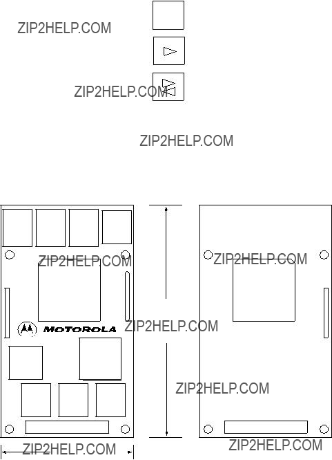
10.0 Gateway Board Physical Layout

Figure 6: Physical Layout (Actual Size)

2 in.

MOTOROLAGATEWAY BOARD15

For More Information On This Product,

Go to: www.freescale.com

Freescale Semiconductor, Inc.

Freescale Semiconductor, Inc.

11.0 Gateway Board Bill Of Material

Table 5: Bill Of Material

16GATEWAY BOARDMOTOROLA

For More Information On This Product,

Go to: www.freescale.com

Freescale Semiconductor, Inc.

12.0 ColdFire Gateway Board Schematics (1 of 2)

U1

MCF5202

0.01UF

Freescale Semiconductor, Inc.

ISPEN GND

10 PF

VCC GND

33 UF

VCC GND

0.1 UF

VCC GND

0.1 UF

VCC GND

0.1 UF

VCC GND

0.1 UF

VCC GND

0.1 UF

VCC GND

0.1 UF

VCC GND

0.1 UF

VCC GND

0.1 UF

VCC GND

0.1 UF

VCC GND

0.1 UF

VCC GND

0.1 UF

VCC GND

0.1 UF

VCC GND

0.1 UF

VCC GND

0.1 UF

VCC GND

0.1 UF

VCC GND

0.1 UF

VCC GND

0.1 UF

VCC GND

0.1 UF

VCC GND

0.1 UF

VCC GND

0.1 UF

BYPASS FOR U1

FOR U2 - U9

VCC GND

0.1 UF

VCC GND

0.1 UF

VCC GND

BYPASS

MOTOROLAGATEWAY BOARD17

For More Information On This Product,

Go to: www.freescale.com

Freescale Semiconductor, Inc.

ColdFire Gateway Board Schematics (2 of 2)

Freescale Semiconductor, Inc.

U2

ISPLSI-1016

U6

74F543

18GATEWAY BOARDMOTOROLA

For More Information On This Product,

Go to: www.freescale.com

Freescale Semiconductor, Inc.

Freescale Semiconductor, Inc.

convey any license under its patent rights nor the rights of others. Motorola products are not designed, intended, or authorized for use as components in systems intended for surgical implant into the body, or other applications intended to support or sustain life, or for any other application in which the failure of the Motorola product could create a situation where personal injury or death may occur. Should Buyer purchase or use Motorola products for any such unintended or unauthorized application, Buyer shall indemnify and hold Motorola and its of???cers, employees, subsidiaries, af???liates, and distributors harmless against all claims, costs, damages, and expenses, and reasonable attorney fees arising out of, directly or indirectly, any claim of personal injury or death associated with such

MOTOROLAGATEWAY BOARD19

For More Information On This Product,

Go to: www.freescale.com