SERVICE
MANUAL
VHF/UHF ALL MODE TRANSCEIVER
i910H
SERVICE
MANUAL
VHF/UHF ALL MODE TRANSCEIVER
i910H

This service manual describes the latest service information for the
To upgrade quality, any electrical or mechanical parts and internal circuits are subject to change without notice or obligation.
NEVER connect the transceiver to an AC outlet or to a DC power supply that uses more than 16 V. This will ruin the transceiver.
DO NOT expose the transceiver to rain, snow or any liquids.
DO NOT reverse the polarities of the power supply when connecting the transceiver.
DO NOT apply an RF signal of more than 20 dBm (100 mW) to the antenna connector. This could damage the transceiv- er???s front end.
ORDERING PARTS
Be sure to include the following four points when ordering replacement parts:
1.
2.Component part number and name
3.Equipment model name and unit name
4.Quantity required
<SAMPLE ORDER>
Addresses are provided on the inside back cover for your convenience.
REPAIR NOTES
1.Make sure a problem is internal before disassembling the transceiver.
2.DO NOT open the transceiver until the transceiver is disconnected from its power source.
3.DO NOT force any of the variable components. Turn them slowly and smoothly.
4.DO NOT short any circuits or electronic parts. An insu- lated tuning tool MUST be used for all adjustments.
5.DO NOT keep power ON for a long time when the trans- ceiver is defective.
6.DO NOT transmit power into a signal generator or a sweep generator.
7.ALWAYS connect a 50 dB to 60 dB attenuator between the transceiver and a deviation meter or spectrum ana- lyzer when using such test equipment.
8.READ the instructions of test equipment thoroughly before connecting equipment to the transceiver.

TABLE OF CONTENTS
SECTION 10 BLOCK DIAGRAMS
10 - 1 MAIN UNIT . . . . . . . . . . . . . . . . . . . . . . . . . . . . . . . . . . . . . . . . . . . . . . . . . . . . . . . . . . . . . . . . . . . . 10 - 1 10 - 2 PA AND PLL UNITS . . . . . . . . . . . . . . . . . . . . . . . . . . . . . . . . . . . . . . . . . . . . . . . . . . . . . . . . . . . . . 10 - 2 10 - 3 FRONT UNIT . . . . . . . . . . . . . . . . . . . . . . . . . . . . . . . . . . . . . . . . . . . . . . . . . . . . . . . . . . . . . . . . . . 10 - 3 10 - 4
SECTION 11 WIRING DIAGRAM
SECTION 12 VOLTAGE DIAGRAMS
12 - 1 FRONT UNIT . . . . . . . . . . . . . . . . . . . . . . . . . . . . . . . . . . . . . . . . . . . . . . . . . . . . . . . . . . . . . . . . . . 12 - 1 12 - 2 PLL UNIT . . . . . . . . . . . . . . . . . . . . . . . . . . . . . . . . . . . . . . . . . . . . . . . . . . . . . . . . . . . . . . . . . . . . . 12 - 2 12 - 3 PA UNIT (1) . . . . . . . . . . . . . . . . . . . . . . . . . . . . . . . . . . . . . . . . . . . . . . . . . . . . . . . . . . . . . . . . . . . . 12 - 3 12 - 4 PA UNIT (2) . . . . . . . . . . . . . . . . . . . . . . . . . . . . . . . . . . . . . . . . . . . . . . . . . . . . . . . . . . . . . . . . . . . . 12 - 4 12 - 5 MAIN UNIT (1) . . . . . . . . . . . . . . . . . . . . . . . . . . . . . . . . . . . . . . . . . . . . . . . . . . . . . . . . . . . . . . . . . 12 - 5 12 - 6 MAIN UNIT (2) . . . . . . . . . . . . . . . . . . . . . . . . . . . . . . . . . . . . . . . . . . . . . . . . . . . . . . . . . . . . . . . . . 12 - 6 12 - 7 MAIN UNIT (3) . . . . . . . . . . . . . . . . . . . . . . . . . . . . . . . . . . . . . . . . . . . . . . . . . . . . . . . . . . . . . . . . . 12 - 6 12 - 8

SECTION 1 SPECIFICATIONS
??? GENERAL
???Mode
???No. of memory Ch.
???Antenna connector
???Usable temp. range
???Frequency stability
???Frequency resolution
???Power supply
???Current drain (at 13.8 V DC)
???Dimensions
(projections not included)
???Weight (approx.)
???ACC 1 connector
???
???DATA connectors
??? TRANSMITTER
???Output power
???Modulation system
???Spurious emission
???Carrier suppression
???Unwanted sideband suppression
???Microphone connector
???KEY connector
*1 Optional
*2 Guaranteed range is
:USB, LSB, CW, FM,
*Not available in 1200 MHz band
:212 (99 regular, 6 scan edges, 1 calls for each band) plus 10 satellite memories)
:
:
:Less than ??3 ppm
:1 Hz minimum
:13.8 V DC ??15% (negative ground)
:
:241(W) ??? 94(H) ??? 239(D) mm 91???2(W) ??? 311???16(H) ??? 913???32(D) in
:4.5 kg; 10 lb (with
:
:
:
: (continuously adjustable)
:More than 40 dB
:More than 40 dB
:
:
All stated specifications are subject to change without notice or obligation.
1 - 1
??? RECEIVER
1 - 2

1 - 2
* Located under side of the point
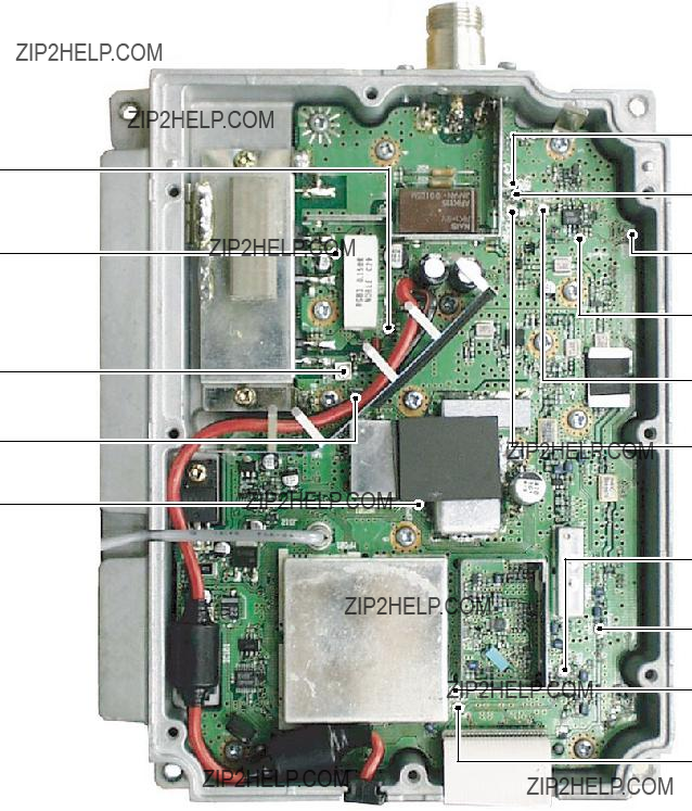
MAIN unit
Crystal band pass filter (FI151:
TX IF amplifier* (Q1: 3SK131)
Crystal band pass filter (FI751:
FM IF IC
(IC951: TA31136FN)
D/A converter (IC1521: M62352GP)
AF power amplifier (IC1852: LA4445)
Analog master IC* (IC1701:
FM IF IC
(IC401: TA31136FN)
PLL unit
DDS gate array (IC331:
430 MHz band VCO circuit
DDS IC
(IC601:
Driver IC
(IC1: BU4094BCF)
 Reference oscillator (X512:
DDS gate array (IC131:
144 MHz band VCO circuit
DDS IC
(IC701:
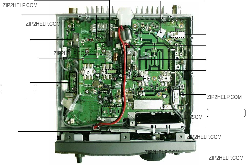
2 - 2
TX/RX switching relay (RL700: AE5349)
RX balanced mixer (Q511, Q512: 2SK1740)
145 MHz power amplifier (Q651, Q652: 2SC5152)
TX balanced mixer Q501, Q502: 2SK302 D502: 1SV286
DRV board
UNIT PA ???
RX balanced mixer (Q220, Q221: 2SC3356)
440 MHz power amplifier (Q151, Q152: 2SC3102)
TX balanced mixer* (Q1, Q2: 2SK302)

 TX double balanced mixer
D190: HSB88WS
L190, L191:
Drive amplifier (Q131: SRFJ7044)
* Located under side of the point

??? TOP VIEW
Power module IC (IC21:
YGR amplifier (IC141: ???PC1878G)
PLL IC
(IC501: TB31242)
1st LO VCO circuit
DDS IC
(IC661:
??? BOTTOM VIEW
Power supply circuit for
2nd IF amplifier (Q81: 2SC2712)
Power supply circuit for
Q72: DTC144EU
Q73, Q74: 2SC2712
RF
RF amplifier (Q271: 2SC5454)
TX 1st mixer (IC131: ???PC8163TB)
RX 1st mixer (IC241: ???PC2721)
TX 1st IF amplifier (IC111: ???PC2709)
RX 2nd mixer (Q221: 3SK166)
TX 2nd mixer (D82: HSB88WS)
2nd LO VCO circuit
Drive amplifier (Q38: 2SK2855)
Divider
(IC610: TC7W74FU)
Reference amplifier (IC601: TC7SU04F)
2 - 3

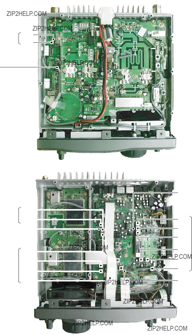
SECTION 3 DISASSEMBLY AND OPTION INSTRUCTIONS
??? Opening the transceiver???s case
Follow the case and cover opening procedures shown here when you want to install an optional unit or adjust the internal units, etc.
qRemove the 5 screws from the top of the trans- ceiver and 4 screws from the sides, then lift up the top cover.
w Turn the transceiver upside down.
eRemove 5 screws from the bottom of the trans- ceiver, then lift up the bottom cover.
CAUTION: DISCONNECT the DC power cable from the transceiver before performing any work on the transceiver. Otherwise, there is a danger of electric shock and/or equipment damage.
Disconnect the 
 speaker cable.
???
q Remove the bottom cover as shown above.
wRemove the antenna plate from the chassis using a stan- dard screw driver.
WARNING!
NEVER attempt to remove the antenna plate using your finger, this may result in injury.
e Connect the FFC (Flexible Flat Cable) of the
CAUTION
NEVER catch the cables from the optional DSP unit(s) between chassis and the
Coaxial cable
PLL unit
J541 
DC power cable
J2 
Flexible flat cable
Power connector
r Place the
BE CAREFUL not to drop the supplied screws inside the transceiver.
Antenna plate
 J2
J2
MAIN unit
Turn the flexible flat cable up under the
t Return the bottom cover to its original position.
3 - 1

??? Opening the PA unit cover
qRemove the top cover as shown in the diagram on p. 3- 1.
wRemove 8 screws and grounding plate from the PA unit cover.
e Remove fastening tape from the inside power cable.
grounding plate
r Slide the PA unit cover as shown below.
???
qRemove the bottom cover as shown in the diagram on p.
??? Remove the
wDisconnect the connection cable connectors from J501 and J1051 on the MAIN unit.
e Remove 2 clips.
WARNING!
BE CAREFUL not to pinch your finger with the clip.
rRemove 6 screws from the MAIN unit, then lift up the MAIN unit.
PLL unit
J501
 J1051
J1051
MAIN unit
Clips
tInstall
ySolder then cut the leads, keeping
u Return the MAIN unit and clips to their original positions.
i
o Return the bottom cover to the original position.
(MAIN)
(SUB)
3 - 2
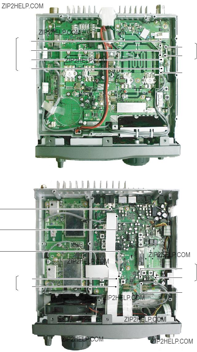
???
qRemove the bottom cover as shown in the diagram on p.
??? Remove the
wRemove the protective paper attached to the bottom of the
ePlug
r Return the bottom cover to its original position.
J1801
MAIN unit
???
RECOMMENDATION:
When installing only 1 DSP unit, you can install into either front or rear panel side. However, installing a DSP unit into the front panel side may be easier and also safer.
Installing 1st DSP unit (front panel side)
qRemove the bottom cover as shown in the diagram on p.
??? Remove the
w Remove the shielding plate.
eRemove the connection cable from J1751 on the MAIN unit. Connect the cable into J1 on the
rPlug the connection cable (P1) from the
tPlug the flat cable into J3 on the
???Take care of the conductor direction.
???Attach the Velcro tape to the
yReturn the shielding plate, top cover and bottom cover to their original positions.
Installing 2nd DSP unit (rear panel side)
qRemove the top and bottom cover as shown in the dia- gram on p.
??? Remove the
w Remove the shielding plate.
eRemove the connection cable from J1761 on the MAIN unit. Connect the cable into J1 on the
The cable between J1221 on the MAIN and J1 on the DSP unit, must be set in the groove of the chassis (see diagram below).
Otherwise, the cable may be damaged when returning the shield plate to its original position.
rPlug the connection cable (P1) from the
tPlug the flat cable into J3 on the
???Take care of the conductor direction.
???Attach the Velcro tape to the
yReturn the shielding plate, top cover and bottom cover to their original positions.
Set cable into the groove.
J1
Shielding plate
PLL unit
J3  J1
J1
J1781 
 P1
P1 
J1761
Take care of the conductor direction.
MAIN unit
3 - 3

???
qRemove the bottom cover as shown in the diagram on p.
??? Remove the
wRemove 6 screws from the PLL shield cover, then lift up the PLL shield cover.
PLL shield cover
eDisconnect the FFC (Flexible Flat Cable) from the DIS- PLAY unit and the connection cable connectors from J501 and J1051 on the MAIN unit.
rRemove 5 screws from the PLL unit, then lift up the PLL unit.
tUnsolder the original reference crystal, then remove it.
???The original reference crystal unit is soldered at both top and bottom sides of the PCB (Printed Circuit Board).
Original crystal
 J501
J501
 J1051
J1051
Flexible flat cable
y Install the
uReturn the PLL unit, PLL shield cover and bottom cover to their original positions.
Original crystal soldering point
3 - 4
SECTION 4 CIRCUIT DESCRIPTION
Note: [Main]=Main band, [Sub]=Sub band
CIRCUIT (PA UNIT)
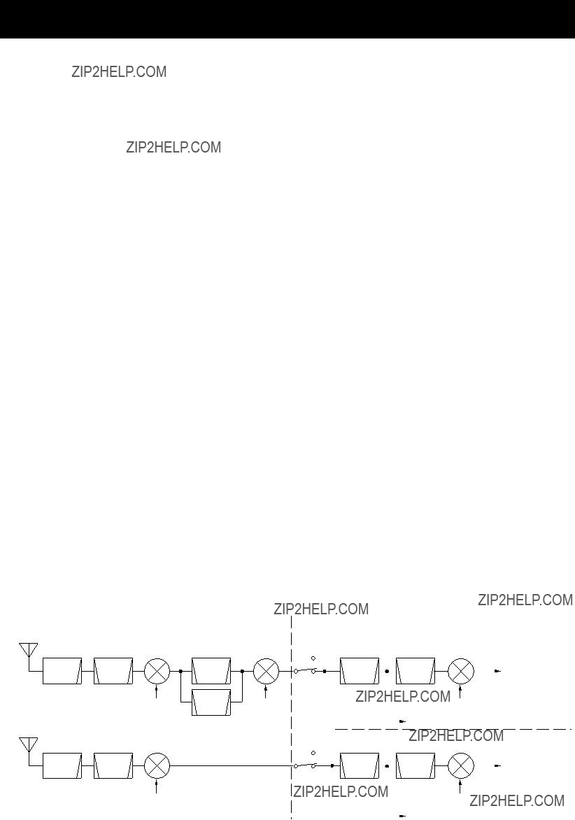
Received signals from the antenna connector (CHASSIS; J1) are passed through the
The transmit/receive switching circuit leads receive signal to the RF circuit from a
The passed signals are then applied to the RF amplifier cir- cuit.
Received signals from transmit/receive switching circuit are applied to the RF amplifier circuit (Q507) via the RF attenu- ator (D515), limiter (D514) and tunable band pass filter (D513, L560) circuits.
The amplified signals are then passed through the another
The 1st mixer circuit converts the received signals into a fixed frequency of the 10 MHz IF signal with a PLL output frequency. By changing the PLL frequency, only the desired frequency will pass through a pair of crystal filters at the next stage of the VHF 1st mixer.
The filtered signals from the bandpass filter are mixed with 1st LO signals at the mixer circuit (Q511, Q512) to produce a 1st IF signal (10.85 MHz [Main] or 10.95 MHz [Sub]). The 1st LO signals (125.15
The 1st IF signal is then applied to either the Main or Sub band 10 MHz IF circuit in the MAIN unit via P501 [Main] or P510 [Sub].
The received signals from the UHF antenna connector (CHASSIS; J2) are passed through the
The filtered RF signals from the bandpass filter are mixed with a 1st LO signal at the 1st mixer circuit (Q220, Q221) to produce a 1st IF signal (71.25 MHz [Main] or 71.35 MHz [Sub]). The 1st IF signal is passed through a crystal filter (Fl280 [Main], Fl281 [Sub]) to suppress
The 1st LO signal (348.75
1st LO A1LO
4 - 1
The 10 MHz IF signal from the mixer circuit is passed through a monolithic filter (Fl51 [Main], Fl651 [Sub]) to sup- press
The amplified signal is then applied to the different circuits depending on the selected mode.
(1) FM mode
The signal is applied to an FM IF IC pin 16 (IC401 [Main] or IC951 [Sub]).
(2) SSB and CW mode
The signal is passed through a 10 MHz IF filter (FI151/10.85 MHz [Main] or Fl751/10.95 MHz [Sub]) or optional CW nar- row filters. The filtered signal is amplified at the IF amplifiers
(1) FM mode
The 10 MHz IF signal from an IF amplifier (Q51 [Main] or Q651 [Sub]) is applied to the mixer section of the FM IF IC (IC401 [Main], IC951 [Sub], pin 16), and is mixed with a LO signal (10.395 MHz [Main], 10.495 MHz [Sub]) to produce a 455 kHz IF signal. The LO signal is generated by the BFO circuit (PLL unit; IC601 [Main], IC701 [Sub]).
The FM detector circuit employs the quadrature detection method, which uses a ceramic discriminator (X401 [Main], X951 [Sub]) for phase delay to obtain a
The detected signals are output from pin 9, and applied to the squelch control and center indication detector circuits, etc.
(2) SSB and CW modes
The amplified signal from the IF amplifier circuit (Q51 [Main], Q651 [Sub]) is applied to the balanced mixer circuit (IC351 [Main], IC851 [Sub]) to demodulate into AF signals. Demodulated audio signals are output from pin 1, and applied to the squelch control gate (IC452 [Main], IC1002 [Sub]).
BFO circuit (PLL unit; IC601 [Main] and IC701 [Sub]) gener- ates BFO signals for using in the balanced mixers.
??? BFO frequencies
The demodulated AF signals from the balanced mixer circuit or FM IF IC are applied to the squelch control gate (IC452 [Main], IC1002 [Sub]). This consists of 4 analog switches which are selected with a mode signal and squelch control signal from the CPU (DISPLAY board; IC1) via the expander IC (IC1491). The switched AF signals are applied to the AF circuit.
(1) FM mode
A squelch circuit cuts out AF signals when no RF signal is received or the
A portion of the AF signals from the FM IF IC pin 9 (IC401 [Main], IC951 [Sub]) passes through the active filter section of FM IFIC (pin 8). The active filter section amplifies and fil- ters noise components. The filtered signals are applied to the noise detector section for conversion into DC voltage and output from pin 14 (IC401 [Main], IC951 [Sub]) as the ???NSQM [Main]/NSQS [Sub]??? signal. The ???NSQM [Main]/ NSQS [Sub]??? signal is applied to the DISPLAY board.
The DC voltages are passed through the analog multiplexer (DISPLAY board; IC5, pins 15 and 2) and then applied to the CPU (DISPLAY board; IC1, pins 93, 94) via the MP1Y and MP1X signal lines. The [SQL] level signal is also applied to the CPU via the analog multiplexer (DISPLAY board; IC3, pins 14, 5) as a reference voltage for comparison with the noise signals. Also, an
(2) SSB and CW modes
The squelch circuit mutes audio output when the
A portion of the 10 MHz IF signal from the IF amplifier (Q352 [Main], Q852 [Sub]) is converted into DC voltage at the AGC detector (D303, Q305 [Main], D902 Q901 [Sub]) and ampli- fied at the meter amplifier (IC1804d [Main] or IC1804b [Sub]). The amplified signal is passed through the analog multiplexer (DISPLAY board; IC4, pins 12 and 1) via the SMLM [Main]/ SMLS [Sub] signals and then applied to the CPU (DISPLAY board; IC1). The CPU outputs control sig- nals to the squelch control gate when the
The AF amplifier circuit amplifiers the demodulated signals to drive a speaker. For the separate speaker function, a stereo power amplifier is used.
AF signals from the squelch control gate are passed through the AF filter (IC451a [Main], IC1001a [Sub]) and AF pre- amplifier (IC451b [Main], IC1001b [Sub]) and then amplified at the voltage controlled amplifier (VCA: IC1808 [Main], IC1809 [Sub]) which functions as a volume control using the [AF] control signal. The amplified AF signals are applied to the AF power amplifier circuit (IC1852, pin 2 [Main], pin 5 [Sub]).
The amplified audio signals of SUB band are output from pin 7, and are applied to the external speaker jack for the SUB band (J1852) via the [PHONE] jack (JACK board; J1). When no plug is connected to the jack, the signals are fed back to the MAIN band audio. The mixed audio is applied to the internal speaker via the [PHONE] jack and external speaker jack for the MAIN band (J1851).
4 - 2

The noise blanker circuit detects
A portion of the 10 MHz IF signal from the bandpass filter (FI51 [Main], FI651 [Sub]) is amplified at the noise amplifier circuit (Q102, IC101, Q101 [Main], Q702, IC701, Q701 [Sub]). The amplified signal is rectified at the noise detector (D371 [Main], D701 [Sub]) for conversion into DC voltage. The DC voltage is amplified at the DC amplifier circuit (Q105 [Main], Q705 [Sub]) and then applied to the noise blanker control circuit (Q52, Q107 [Main], Q652, Q707 [Sub]) to stop amplification of the IF amplifier circuit (Q51 [Main], Q651 [Sub]).
The AGC (Auto Gain Control) circuit reduces IF amplifier gain to keep the audio output at a constant level.
A portion of the 10 MHz IF signal from the IF amplifier (Q352 [Main], Q852 [Sub]) is applied to the AGC detector circuit D303 [Main], D902 [Sub]). The detected signal is then ampli- fied at the DC amplifier circuit (Q305 [Main], Q901 [Sub]) and then applied to the IF amplifiers (Q51, Q351, Q352 [Main], Q651, Q851, Q852 [Sub]).
When strong signals are received, the detected voltage increases and the output level of the DC amplifier, as AGC voltage, decreases. The AGC voltage is used for the bias voltage for the IF amplifiers, therefore, the IF amplifier gain is decreased.
AGC response time is controlled by changing the time con- stant at the AGC control line with a resistor and capacitor. While AGC is set to slow, the resistor (R312 [Main], R914 [Sub]) and capacitor (C306 [Main], C911 [Sub]) are con- nected to the AGC control line. While AGC is set to fast, R311 [Main], R913 [Sub] are connected to the AGC control line. Due to Q304 and Q303 [Main]/Q905 and Q904 [Sub] being switched ON that controlled by the ???AGSM???, ???AGFM??? [Main], ???AGSS???, ???AGFS??? [Sub]. Also, R310 [Main]/R912 [Sub] is connected to the AGC control line due to Q302 [Main]/Q903 being switched ON while scanning for faster response than AGC fast mode that controlled by the ???AGRM??? [Main], ???AGRS??? [Sub].
The
(1) FM mode
Some of the amplified IF signal is applied to the
(2) SSB and CW modes
A portion of the AGC control signal is applied to the meter amplifier (IC1804d [Main], IC1804b [Sub]). The amplified signal is then applied to the CPU via the analog multiplexer to control the
The microphone amplifier circuit amplifies audio signals from the microphone or ACC connector and then applies them to the FM modulation or balanced modulator circuit. One microphone amplifier circuit is commonly used for both FM/SSB and VHF/UHF.
Audio signals from the [MIC] connector enter the micro- phone amplifier IC (IC1701, pin 22) and are then amplified at the microphone amplifier or speech compressor section. Compression level is adjusted by the setting mode.
The amplified or compressed signals are applied to the VCA section of IC1701. The microphone gain setting from the D/A converter (IC1521, pin 8) is applied to the VCA control ter- minal (IC1701, pin 10). The resulting signals from pin 9 are then applied to the
??? AGC CIRCUIT FOR MAIN BAND
D302
RFGM  (RF/SQL control)
9 V 
4 - 3
While in SSB mode, the amplified signals from the buffer amplifier (Q1651) are then applied to the balanced modula- tor (IC201).
While in AM/FM mode, the amplified signals from the buffer amplifier (Q1651) are applied to the limiter amplifier (IC1651b) and splatter filter (IC1651a). The signals are passed through the buffer amplifier ((IC1652a) and are then applied to the AM detector (IC1807d, D1652) in AM mode or to the varactor diode (D253) in FM mode.
The modulated IF signal from a modulation circuit is applied to the IF amplifier circuit (Q1). The amplified IF signal is then applied to the VHF/UHF transmit circuit (PA unit) via the VHF /UHF switching circuit (D52, D53).
The gain of the IF amplifier circuit (Q1) is controlled by the ALC amplifier circuit (IC1601b). Therefore, the IF amplifier is reduced when the output power increases.
(1) FM mode
The amplified audio signals from IC1701 are
The FM modulation circuit changes the generating frequen- cy of the FM local oscillator (Q254, X251) to generate an FM signal. The modulated IF signal is passed through the RF limiter (Q253) and then applied to the transmit IF amplifier circuit.
When 9600 bps mode is selected, audio signals from the ACC connector bypass the amplifiers and are applied to IC1654a directly via the external modulation switch (IC1531, pins 12, 1). In such cases, the deviation detector (IC1807d) cuts off the audio line when over modulation is detected.
(2) SSB and CW modes
The amplified audio signals from Q1651 are mixed with BFO signals at the balanced mixer circuit (IC201) to produce a 10 MHz IF signal. The mixed signal is still a DSB signal, there- fore, the mixed signal passes through bandpass filter circuit (FI151) to suppress unwanted side band signals. The fil- tered signal is applied to the transmit IF amplifier circuit
??? Transmit IF frequencies
When the CW key is closed, control signal is output from CPU (LOGIC unit) and controls
Keying signals (DOT and DASH) from the [KEY] jack (J1401) are applied to the CPU (DISPLAY board; IC1, pins 49, 48 respectively), and the CPU outputs a CW control sig- nal (KDS1) from pin 21. The CW control signal is applied to the balanced mixer (IC201) via Q201, D201, D207 to unbal- ance the IC201 input bias voltage and creates a carrier sig- nal. R202 determines the transmit delay timing.
The RF circuit consists of mixer and drive amplifiers to obtain the desired frequency and level needed at a PA cir- cuit, respectively.
(1) VHF band
The IF signal from the MAIN unit (P501) is mixed with an LO signal from the VHF VCO circuit (PLL unit; Q191,
The amplified and filtered RF signal is applied to the drive amplifier circuit that is used VHF and UHF signals common- ly.
(2) UHF band
The IF signal from the MAIN unit (P1) is mixed with a 2nd LO signal at the
The 1st mixer circuit (D190, L190, L191) converts the 2nd IF signal into a UHF transmit frequency with a 1st LO signal from the UHF VCO circuit (PLL unit; Q391,
The drive amplifier circuit amplifies RF signals from the VHF or UHF RF circuit to obtain a level needed at the power amplifier circuit. One drive amplifier circuit is commonly used for both VHF and UHF band signals.
The signals from the VHF or UHF RF circuit are amplified at the drive amplifier circuit (Q101, Q121, Q131, DRV board; Q930). The amplified VHF signals are passed through the
4 - 4
The power amplifier circuit amplifies the RF signals to the specified output power.
(1) VHF power amplifier circuit
The RF signal from the
(2) UHF power amplifier circuit
The RF signal from the
The ALC (Automatic Level Control) circuit protects the power amplifiers (PA unit; Q651, Q652 for VHF and Q151, Q152 for UHF) from a mismatched output load. Also, the ALC circuit controls the gain of the transmit IF amplifier in order for the transceiver to output even when the supplied voltage shifts, etc.
The RF power level is detected at the power detector circuit (PA unit;
When the VFOR/UFOR voltage increased, the output from the differential amplifier will be decrease to reduce the IF amplifier gain. This adjusts the RF output power until the VFOR/UFOR and POCV voltage are well balanced.
The VHF PLL circuit generates the 1st LO frequency, and the signal is applied to the VHF 1st mixer circuit in the PA unit as the ???A1LO??? signal. The PLL circuit consists of a VCO, prescaler and DDS circuits.
The signal generated at the VHF VCO circuit (Q191,
The output pulses are converted into DC voltage at the loop filter circuit (IC161a) and then applied to the VHF VCO cir- cuit.
The D/A converter
The UHF PLL circuit generates the 1st LO frequency, and the signal is applied to the UHF 1st mixer circuit in the PA unit as the ???B1LO??? signal. The PLL circuit consists of a VCO, prescaler and DDS circuits.
The signal generated at the UHF VCO circuit (Q391,
The D/A converter
The APC (Automatic Power Control) circuit protects the power amplifiers on the PA unit from excessive current.
Current drain of power amplifiers is detected by voltage drops at a resistor (PA unit; R305) between VCC and PAHV lines. The original voltage (ICH) and dropped voltage (ICL) are applied to the APC differential amplifier (MAIN unit; IC1601d).
The signal output from the differential amplifier reduces IF amplifier gain until these voltages are
Received signals from the antenna connector (CHASSIS; J501) are applied to the transmit/receive switching circuit (RL51).
The transmit/receive switching circuit leads receive signal to the RF circuit while receiving. However, the circuit leads the transmit signal from the RF power amplifier to the antenna connector while transmitting.
4 - 5
The passed signals are then applied to the RF amplifier cir- cuit.
Received signals from the transmit/receive switching circuit are passed through the
The amplified signals are then passed through the another bandpass filter (FI271) to suppress unwanted signals. The filtered signals are then applied to the 1st mixer circuit (IC241).
The 1st/2nd mixer circuits convert the received signals into a fixed frequency of the 10 MHz IF signal with a PLL output frequencies. By changing the PLL frequency, only the desired frequency will pass through a filter at the next stage.
The filtered signals from the bandpass filter are mixed with 1st LO signals at the mixer circuit (IC241) to produce a 1st IF signal (243.95 MHz). The 1st LO signals (996.0
The 1st IF signal is passed through the bandpass filter (FI241) to suppress unwanted signals, and then applied to the 2nd mixer circuit (Q221).
The applied signal is mixed with 2nd LO signal coming from the 2nd LO VCO circuit (Q731) to produce a 10.85 MHz [Main], 10.95 MHz [Sub] 2nd IF signal. The 2nd IF signal is passed through the main/sub switching circuit (Q161, Q164), and then output to the MAIN unit of
The amplified signals are passed through the bandpass fil- ter (FI1) to suppress spurious components, and are ampli- fied at the
The output signals from the power module (IC21) are passed through the duplexer circuit (RL51) and detector cir- cuits of forwared voltage and refrected voltage, and are then applied to the antenna connector.
The reference frequency from the
The 1LO PLL circuit generates the 1st LO frequency, and the signal is applied to the 1st mixer circuit as the ???1LO??? sig- nal.
An oscillated signal from the 1LO VCO (Q541, Q542) pass- es through the buffer amplifiers (Q551, Q681) and is applied to the PLL IC (IC501, pin 1) and is prescaled in the PLL IC based on the divided ratio
The modulated 2nd IF signal from
The applied signal is mixed at the 2nd mixer circuit (D82, L84, L85) to converted into the 1st LO signal with the 2nd LO signal, which comes from the 2nd LO VCO (Q731).
Then the 1st LO signal is passed through the
The signal is mixed with the 1st LO signal coming from the 1st LO VCO circuit (Q451, Q452) to converted into RF sig- nals.
The RF signals from the 1st mixer circuit are passed through the bandpass filter (FI141) and
The 2LO PLL circuit generates the 2nd LO frequency, and the signal is applied to the 2nd mixer circuit as the ???2LO??? sig- nal.
The signal generated at the 2LO VCO circuit (Q731) is amplified at the buffer amplifiers (Q741, Q761), then applied to the prescaler circuit (IC761). The prescaler circuit divides the applied signal, and outputs it to the DDS circuit (IC661) via the buffer amplifier (Q762). The DDS circuit generates digital signals using the applied signals as a clock frequen- cy. The phase detector section in IC661 compares its phase with the reference frequency from the reference amplifier (IC601). IC661 outputs
The output pulses are converted into DC voltage at the loop filter circuit (IC701a) and then applied to the 2LO VCO cir- cuit.
The D/A converter
4 - 6

SECTION 5 ADJUSTMENT PROCEDURES
??? REQUIRED TEST EQUIPMENT
??? CONNECTIONS
CAUTION !
DO NOT transmit while an SSG is connected to the antenna connector.
Standard signal generator
Audio generator
,.
[MIC]
PTT
CAUTION !
When [P.AMP] switch is turned ON, DC voltage is applied to the antenna connector. This may damege the signal generator.
JIG cable (B)
+9 V
 2.2 k
2.2 k
5 - 1

After adjustment, connect P501, P502 (PA unit) to J51, J52 on the MAIN.
5 - 2
??? PLL AND MAIN UNITS
R570
30.2 MHz level adjustment
L193
144M lock voltage adjustment
P251
144M LO level check point
X512
Reference frequency adjustment
J541
30.2 MHz level check point
Main BFO level check point
P701
Sub BFO level check point
CP100
144M lock voltage check point
P551
Reference frequency check point
L255
FM
CP51
FM
5 - 3
Receiver adjustments must be performed after software adjustment (0) and (1). SUB band must be OFF when adjusting MAIN band, or main AF volume (max.counter clockwise) and SQL volume (max. clockwise) must be set when adjusting SUB band.
*This output level of a standard signal generator (SSG) is indicated as SSG???s open circuit.
5 - 4
??? PA UNIT
adjustment L521
P501
144M receiver peak/gain check point
??? MAIN UNIT
R857
144M total gain adjustment
for sub band
L853
L852
L851 144M peak adjustment
L653 for sub band
L652
L651
J51
144M receiver peak/gain
5 - 5

RECEIVER ADJUSTMENTS (continued)
100msec.
1msec.
???Receiving
*This output level of a standard signal generator (SSG) is indicated as SSG???s open circuit.
5 - 6
??? PA UNIT
L283
430M peak
adjustment L282 for main band L23
L22
??? MAIN UNIT
CP851
430M peak check point for main band
CP852
430M peak check point for sub band
CP101
Noise blanker check point for main band
for main band L103
R61
430M total gain adjustment
for main band
L703 Noise blanker adjustment
L704 for sub band
CP701
Noise blanker check point for sub band
5 - 7
3 ??? Repeat step 1, step 2 several times.
5 - 8

??? PA UNIT
P501
RF peak
R503
PA unit
C659
RF peak adjustment for 430M
RF peak
R150
Idling current adjustment for 430M
??? MAIN UNIT
R206 Carrier suppression
R215 adjustment
5 - 9

TRANSMITTER ADJUSTMENTS (continued)
After adjustment, connect P501 (PA unit) to J51 on the MAIN.
???Connect an audio generator to [MIC] connector and set as:
???Connect an audio generator to [MIC] connector and set as:
After adjustment, disconnect CP1631 (PA unit) from GND on the MAIN.
???Disconnect P501 (PA unit) from J51 on the MAIN unit.
???Connect an audio generator to [MIC] connector and set as:
???Connect a keyer to the [KEY] jack.
???Key down (transmitting)
After adjustment, connect P501 (PA unit) to J51 on the MAIN.
5 - 10

??? MAIN UNIT
??? PA UNIT
P501
IF total gain /Drive level
R503
Total gain adjustment for 144M
R504
LO leak
adjustment for 144M
R202
Drive level adjustment
 CP1613
IC APC
R1613
IC APC adjustment
R3
IF total gain adjustment
J51
IF total gain /Drive level check point
R3
Total gain adjustment for 430M
5 - 11

CAUTION:
NEVER select ajustment items
*This output level of a standard signal generator (SSG) is indicated as SSG???s open circuit.
5 - 12
SOFTWARE ADJUSTMENT (continued)
*This output level of a standard signal generator (SSG) is indicated as SSG???s open circuit.
5 - 13

SOFTWARE ADJUSTMENT (continued)
*This output level of a standard signal generator (SSG) is indicated as SSG???s open circuit.
5 - 14

SOFTWARE ADJUSTMENT (continued)
*This output level of a standard signal generator (SSG) is indicated as SSG???s open circuit.
5 - 15

SOFTWARE ADJUSTMENT (continued)
*This output level of a standard signal generator (SSG) is indicated as SSG???s open circuit.
5 - 16

SOFTWARE ADJUSTMENT (continued)
5 - 17
*This output level of a standard signal generator (SSG) is indicated as SSG???s open circuit.
5 - 18
CP321
Idling check point
CP322
Idling check point
C332
Power ballance adjustment
R13
Idling adjustment
CP501
1st LO lock voltage check point
R67
APC adjustment
CP401
APC check point
CP15
APC check point
R288
Attenuator adjustment
R37
APC adjustment
R61
APC adjustment
R83
Transmitter gain adjustment
R224
Receiver gain adjustment
CP701
2nd LO lock voltage check point
CP311
Receiver gain check point
5 - 19

*This output level of a standard signal generator (SSG) is indicated as SSG???s open circuit.
5 - 20

R67
APC adjustment
CP401
APC check point
CP15
APC check point
R37
APC adjustment
R61
APC adjustment
CP311
APC adjustment
5 - 21

[DISPLAY BOARD]
S.=Surface mount
6 - 1
[DISPLAY BOARD]
[DISPLAY BOARD]
S.=Surface mount
6 - 2

[DISPLAY BOARD]
[DISPLAY BOARD]
S.=Surface mount
6 - 3

[RIT BOARD]
[PLL UNIT]
S.=Surface mount
6 - 4
[PLL UNIT]
[PLL UNIT]
S.=Surface mount
6 - 5
[PLL UNIT]
[PLL UNIT]
S.=Surface mount
6 - 6
[PLL UNIT]
[PLL UNIT]
S.=Surface mount
6 - 7
[PLL UNIT]
[MAIN UNIT]
S.=Surface mount
6 - 8
[MAIN UNIT]
[MAIN UNIT]
S.=Surface mount
6 - 9
[MAIN UNIT]
[MAIN UNIT]
S.=Surface mount
6 - 10
[MAIN UNIT]
[MAIN UNIT]
S.=Surface mount
6 - 11
[MAIN UNIT]
[MAIN UNIT]
S.=Surface mount
6 - 12
[MAIN UNIT]
[MAIN UNIT]
S.=Surface mount
6 - 13
[MAIN UNIT]
[MAIN UNIT]
S.=Surface mount
6 - 14
[MAIN UNIT]
[MAIN UNIT]
S.=Surface mount
6 - 15
[MAIN UNIT]
[MAIN UNIT]
S.=Surface mount
6 - 16
[PA UNIT]
[PA UNIT]
S.=Surface mount
6 - 17
[PA UNIT]
[PA UNIT]
S.=Surface mount
6 - 18
[PA UNIT]
[PA UNIT]
S.=Surface mount
6 - 19
[PA UNIT]
[PA UNIT]
S.=Surface mount
6 - 20
[PA UNIT]
[PA UNIT]
S.=Surface mount
6 - 21
[PA UNIT]
[PA UNIT]
S.=Surface mount
6 - 22
[PA UNIT]
[PA UNIT]
S.=Surface mount
6 - 23

[PA UNIT]
[DRV BOARD]
S.=Surface mount
6 - 24
[MAIN UNIT]
[MAIN UNIT] ???
S.=Surface mount
6 - 25
[MAIN UNIT] ???
[MAIN UNIT] ???
S.=Surface mount
6 - 26
[MAIN UNIT] ???
[MAIN UNIT] ???
S.=Surface mount
6 - 27
[MAIN UNIT] ???
[MAIN UNIT] ???
S.=Surface mount
6 - 28
[MAIN UNIT] ???
[MAIN UNIT] ???
S.=Surface mount
6 - 29
[MAIN UNIT] ???
[MAIN UNIT] ???
S.=Surface mount
6 - 30

SECTION 7 MECHANICAL PARTS
[FRONT UNIT]
[DISPLAY UNIT]
[RIT BOARD]
[JACK BOARD]
[MIC BOARD]
[COVER PARTS]
[CHASSIS PARTS]
* Refer to Section 9 BOARD LAYOUTS.
7 - 1
[PA UNIT]
[PLL UNIT]
[MAIN UNIT]
[DRV BOARD]
[UNPACKING]
* Refer to Section 9 BOARD LAYOUTS.
7 - 4

SECTION 8
??? TRANSISTORS AND FET???S
8 - 1
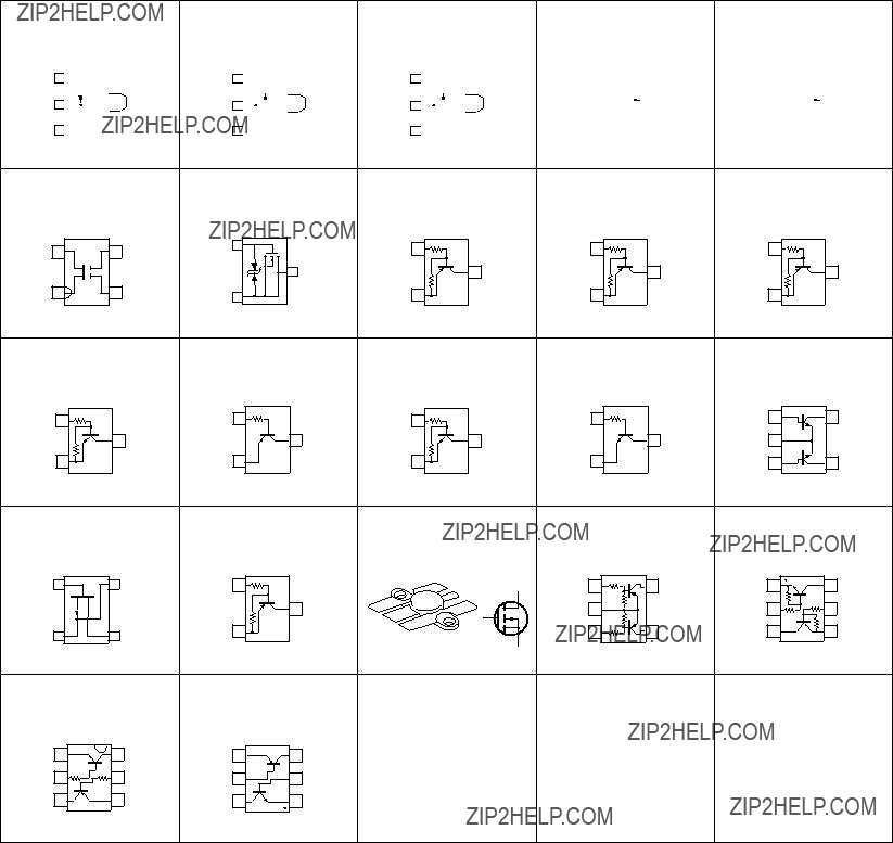
8 - 2

??? DIODES
8 - 3

2 6
J1
GND
NC
MSVR
MAVR
NC
+5V
1 5
to DISPLAY board J2
??? TOP VIEW
to DISPLAY board J10
to DISPLAY board J11
9 - 1

??? BOTTOM VIEW
9 - 2

Icom America Inc.
<Corporate Headquarters>
2380 116th Avenue N.E., Bellevue, WA 98004, U.S.A. Phone : (425)
URL : http://www.icomamerica.com
<Customer Service> Phone : (425)
Icom Canada
Glenwood Centre
Highway 17 Delta, B.C., V4K 5B8, Canada Phone : (604)
Icom (Australia) Pty. Ltd.
A.B.N. 88 006 092 575
URL : http://www.icom.net.au
Icom New Zealand
146A Harris Road, East Tamaki, Auckland, New Zealand
Phone : 09 274 4062 Fax : 09 274 4708
URL : http://www.icom.co.nz
Icom (Europe) GmbH
Communication Equipment
Himmelgeister Str. 100,
URL : http://www.icomeurope.com
Icom Spain S.L
Crta. de Gracia a Manresa Km. 14,750
08190 Sant Cugat del Valles Barcelona, SPAIN Phone : (93) 590 26 70 Fax : (93) 589 04 46 URL : http://www.icomspain.com
Icom (UK) Ltd.
Unit 9, Sea St., Herne Bay, Kent, CT6 8LD, U.K. Phone : 01227 741741 Fax : 01227 741742 URL : http://www.icomuk.co.uk
Icom France S.a
Zac de la Plaine, Rue Brindejonc des Moulinais BP 5804, 31505 Toulouse Cedex, France Phone : 561 36 03 03 Fax : 561 36 03 00 URL :
Asia Icom Inc.
6F No. 68, Sec. 1
