EM78P221/2N
with OTP ROM
Product
Specification
DOC. VERSION 1.0
ELAN MICROELECTRONICS CORP.
October 2007
EM78P221/2N
with OTP ROM
Product
Specification
DOC. VERSION 1.0
ELAN MICROELECTRONICS CORP.
October 2007

Trademark Acknowledgments:
IBM is a registered trademark and PS/2 is a trademark of IBM. Windows is a trademark of Microsoft Corporation.
ELAN and ELAN logo  are trademarks of ELAN Microelectronics Corporation.
Copyright ?? 2007 by ELAN Microelectronics Corporation
All Rights Reserved
Printed in Taiwan
The contents of this specification are subject to change without further notice. ELAN Microelectronics assumes no responsibility concerning the accuracy, adequacy, or completeness of this specification. ELAN Microelectronics makes no commitment to update, or to keep current the information and material contained in this specification. Such information and material may change to conform to each confirmed order.
In no event shall ELAN Microelectronics be made responsible for any claims attributed to errors, omissions, or other inaccuracies in the information or material contained in this specification. ELAN Microelectronics shall not be liable for direct, indirect, special incidental, or consequential damages arising from the use of such information or material.
The software (if any) described in this specification is furnished under a license or nondisclosure agreement, and may be used or copied only in accordance with the terms of such agreement.
ELAN Microelectronics products are not intended for use in life support appliances, devices, or systems. Use of ELAN Microelectronics product in such applications is not supported and is prohibited.
NO PART OF THIS SPECIFICATION MAY BE REPRODUCED OR TRANSMITTED IN ANY FORM OR BY
ANY MEANS WITHOUT THE EXPRESSED WRITTEN PERMISSION OF ELAN MICROELECTRONICS.
ELAN MICROELECTRONICS CORPORATION

Contents
Contents
(This specification is subject to change without further notice)

Contents

Contents
Specification Revision History

EM78P221/2N
Read Me First !
Comparison between
This series of microcontrollers comprise of the older
(This specification is subject to change without further notice)

EM78P221/2N
1 General Description
EM78P221N and EM78P222N are
With its enhanced
2 Features
??CPU configuration
???4K???13 bits
???144???8 bits
???
???3 programmable Level Voltage Reset (LVR) : 4.0V, 3.0V, 2.5V
???Less than 1.5 mA at 5V/4MHz
???Typically 15 ??A, at 3V/32kHz
???Typically 2 ??A, during sleep mode
??I/O port configuration
???4 bidirectional I/O ports: P5, P6, P7 and P8
???
???26 I/O pins
???8 programmable
???8 programmable
???8 programmable
???16 Programmable high sink current I/O pins
???8 Programmable high drive current I/O pins
???External interrupt : P77, P71
??Operating voltage range:
???OTP version:
Operating voltage range: 2.1V~5.5V (commercial)
Operating voltage range: 2.3V~5.5V (industrial)
??Operating temperature range:
Operating temperature range: 0??C~70??C (commercial)
Operating temperature range:
??Operating frequency range
???Crystal mode:
DC~16MHz/2 clks @ 4.5V; DC~125ns inst. cycle @ 4.5V
DC ~ 8MHz/2 clks @ 3V; DC~250ns inst. Cycle
@3V
???ERC mode:
DC ~ 16MHz/2 clks @ 4.5V; DC~125ns inst. cycle @ 5V
DC ~ 8MHz/2 clks @ 3V; DC ~ 250ns inst. Cycle
@3V
???IRC mode:
Oscillation mode: 16MHz, 4 MHz, 1 MHz, 455kHz
Process deviation: Typ ?? 3%, Max. ?? 5%
Temperature deviation: ?? 5%
All these four main frequencies can be trimmed by programming with four calibrated bits in the ICE220N Simulator. OTP is auto trimmed by ELAN Writer (DWTR).
??Fast
Crystal: 4MHz, C1/C2: 30pF) in HXT2 mode and 10??s in IRC mode (VDD:5V IRC:4MHz)
??Peripheral configuration
???
???One comparator (can act as an OP). (offset voltage is smaller than 10mV)
??Five available interrupts
???TCC overflow interrupt
???
???Two External interrupts
???Comparator high/low interrupt
??Special Features
???Programmable free running Watchdog Timer
???Two clocks per instruction cycle
???
???High EFT immunity (better performance at 4MHz or below
???Power saving Sleep mode
???Selectable Oscillation mode
???Package Type:
???
???24 pin SSOP 209mil : EM78P221NAMJ/NAMS
???
(This specification is subject to change without further notice)

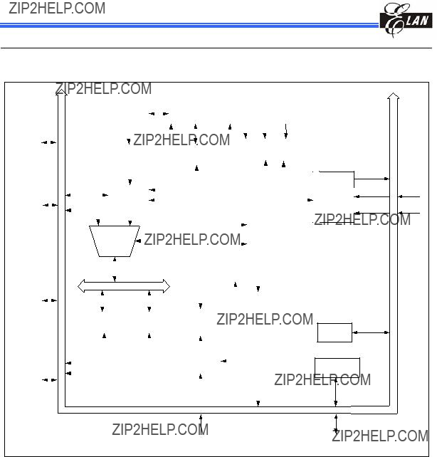
3Pin Assignment
(1)
Fig.
EM78P221/2N
(2)
Fig.
(This specification is subject to change without further notice)

EM78P221/2N
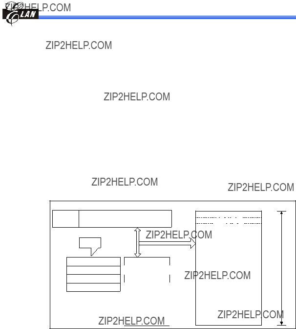
4Pin Description
4.1EM78P222N
(This specification is subject to change without further notice)
EM78P221/2N
4.2 EM78P221N
(This specification is subject to change without further notice)
EM78P221/2N
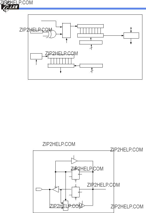
5 Block Diagram
LVR
Comparator
Fig.
(This specification is subject to change without further notice)

EM78P221/2N
6Function Description
6.1Register Configuration
Address
00
01
02
03
04
05
06
07
08
09
0A
0B
0C
0D
0E
0F
10
:
1F
20
:
3F
Note: 1. All registers are 8 bits.
2.When using ICE, some registers code options are set. Refer to Section 6.2 for detailed Registers Description.
3.Registers with * can only be used in ICE220N simulator.
(This specification is subject to change without further notice)

EM78P221/2N
6.2 Registers Description
6.2.1 A (Accumulator)
Internal data transfer operation, or instruction operand holding usually involves the temporary storage function of the Accumulator. The Accumulator is not an addressable register.
Bit 7 (INTE): INT signal edge
0 = interrupt occurs at the rising edge on the INT0 and INT1 pin 1 = interrupt occurs at the falling edge on the INT0 and INT1 pin
Bit 6 (INT): Interrupt enable flag
0 = masked by DISI or hardware interrupt
1 = enabled by the ENI/RETI instructions This bit is readable only.
Bit 5 (TS): TCC signal source
0 = internal instruction cycle clock. If P56 is used as I/O pin, TS must be 0. 1 = transition on the TCC pin
Bit 4 (TE): TCC signal edge
0 = increment if the transition from low to high takes place on the TCC pin 1 = increment if the transition from high to low takes place on the TCC pin.
Bit 3 (PSTE): Prescaler enable bit for TCC
0 = prescaler disable bit. TCC rate is 1:1
1 = prescaler enable bit. TCC rate is set as Bit 2 ~ Bit 0.
Bit 2 ~ Bit 0 (PST2 ~ PST0): TCC prescaler bits
(This specification is subject to change without further notice)
EM78P221/2N
6.2.3 R0 (Indirect Addressing Register)
R0 is not a physically implemented register. Its major function is to perform as an indirect address pointer. Any instruction using R0 as a pointer, actually accesses the data pointed by the RAM Select Register (R4).
6.2.4 R1 (Memory Switch Register)
Bits 7~2: not used bits, fixed to 0 all the time.
Bits 1~0: used to select Banks 0 ~ 3 for R20~R3F and select Banks 0 ~ 3 for the control register.
See the table under Section 6.2 Registers Description for the data memory configuration.
6.2.5 R2 (Program Counter and Stack)
Fig.
R2 and hardware stacks are
Generates 4K???13 bits
The contents of R2 are all set to "0"s when a reset condition occurs.
(This specification is subject to change without further notice)

EM78P221/2N
"JMP" instruction allows direct loading of the lower 10 program counter bits. Thus, "JMP" allows PC to jump to any location within a Page (1K).
"CALL" instruction loads the lower 10 bits of the PC, and then PC+1 is pushed into the stack. Thus, the subroutine entry address can be located anywhere within a page (1K).
"LJMP" instruction allows direct loading of the lower 11 program counter bits. Therefore, "LJMP" allows PC to jump to any location within 2K (212).
"LCALL" instruction loads the lower 11 bits of the PC, and then PC+1 are pushed onto the stack. Thus, the subroutine entry address can be located anywhere within 2K (212).
"RET" ("RETL k", "RETI") instruction loads the program counter with the contents of the top of stack.
"ADD R2, A" allows a relative address to be added to the current PC, and the ninth and above bits of the PC will increase progressively.
"MOV R2, A" allows loading of an address from the "A" register to the lower 8 bits of the PC, and the ninth and above bits of the PC will remain unchanged.
Any instruction (except ???ADD R2,A???) that is written to R2 (e.g., "MOV R2, A", "BC R2, 6" etc.) will cause the ninth bit and above bits of the PC to remain unchanged.
All instructions are single instruction cycle (fclk/2) except ???LCALL??? and ???LJMP??? instructions. The ???LCALL??? and ???LJMP??? instructions need two instructions cycle.
6.2.6 R3 (Status Register)
(This specification is subject to change without further notice)

EM78P221/2N
6.2.7 R4 (Select Indirect Address)
Bits 7~6: not used, fixed to 0 all the time.
Bit 5 ~ Bit 0: used to select registers (Address: 00 ~ 3F) in indirect addressing mode.
6.2.8 Bank
Bits 7 ~ 0 (P57 ~ P50): I/O data bits
6.2.9Bank
Bits 7 ~ 0 (P67 ~ P60): I/O data bits
6.2.10 Bank
Bits 7 ~ 0 (P77 ~ P70): I/O data bits
[With Simulator]: P73 ~ P72 are input or
[With EM78P221/2N]: P73 ~ P72 are general input or output pins.
6.2.11 Bank
Bits 7~6, 4~2, 0: not used, fixed to 0 all the time.
Bit 5 (NREN): Noise rejection enable
0 = disable noise rejection (Default)
1 = enable noise rejection. However in crystal oscillator mode (LXT2), the noise rejection circuit is always disabled.
Bits 1 ~0 (P81~P80): I/O data bit.
6.2.12 Bank
Bits 7~0: not used, fixed to "0" all the time.
(This specification is subject to change without further notice)

EM78P221/2N
6.2.13 Bank
Bit 7 (EX1IF): External interrupt flag. Set by INT1 pin, reset by software. 0 = no interrupt occurs
1 = with interrupt request
Bits 6~5, 3, 1: not used bits, fixed to 0 all the time
Bit 4 (ICWE): Port 6 input change to
When the Port 6 Input Status Change is used to enter interrupt vector or to
Bit 2 (CMPWE): Comparator
0= Disable Comparator
1= Enable Comparator
When the Comparator output status change is used to enter interrupt vector or to
Bit 0 (CMPIF): Comparator interrupt flag. Set when a change occurs in the output of Comparator. Reset by software.
0 = no interrupt occurs
1 = with interrupt request
NOTE
???Bank
???
???Interrupt results from "logic AND" of Bank
6.2.14 Bank
(This specification is subject to change without further notice)

EM78P221/2N
Bit 1 (ICIF): Port 6 input status change interrupt flag. Set when Port 6 input changes. Reset by software.
0 = no interrupt occurs
1 = with interrupt request
Bit 0 (TCIF): TCC overflow interrupt flag. Set when TCC overflows. Reset by software. 0 = no interrupt occurs
1 = with interrupt request
NOTE
???Bank
???
???Interrupt results from "logic AND" of Bank
6.2.15 Bank
Bits 7~0: 0 = defines the relative I/O pin as output
1 = puts the relative I/O pin into high impedance Bank
6.2.16 Bank
Bits 7~2: not used, fixed to 0 all the time
Bits 1~0 (C81~C80): 0 = defines the relative I/O pin as output
1 = puts the relative I/O pin into high impedance
With Simulator]: P80 and P81 are General I/O pins
[With EM78P221/2N]: P80 is General input or output, but P81 is input or
(This specification is subject to change without further notice)

EM78P221/2N
6.2.17 Bank
Bits 7~0: not used, fixed to 0 all the time
6.2.18 Bank
Bit 7 (EIS1): Control bit used to define the function of the P71 (/INT1) pin
0 = P71, normal I/O pin
1 = /INT1, external interrupt pin. In this case, the I/O control bit of P71 (Bit 1 of Bank
Bit 6 (EIS0): Control bit used to define the function of the P77 (/INT0) pin
0 = P77, normal I/O pin
1 = /INT0, external interrupt pin. In this case, the I/O control bit of P77 (Bit 7 of Bank
NOTE
??When EIS is "0," the path of /INT is masked. When EIS is "1," the status of /INT pin can also be read by way of reading Port 7 (Bank
??EIS0 and EIS1 are both readable and writable.
??The highest priority of P71/INT1/CO2 is INT1. When EIS1=0, the working type of P71/INT1/CO is determined by CMPCOS1 and CMPCOS0.
Bit 5 (CMPOUT): The result of the comparator output
Bit 4 ~ Bit 3 (CMPCOS1 ~ CMPCOS0): Comparator Select bits
Bits 2~0: not used, fixed to 0 all the time
(This specification is subject to change without further notice)
EM78P221/2N
6.2.19 Bank
Bank
Bit 7 (/PD7): Control bit used to enable the
0= Enable internal
1= Disable internal
Bit 6 (/PD6): Control bit used to enable the
Bit 5 (/PD5): Control bit used to enable the
Bit 4 (/PD4): Control bit used to enable the
Bit 3 (/PD3): Control bit used to enable the
Bit 2 (/PD2): Control bit used to enable the
Bit 1 (/PD1): Control bit used to enable the
Bit 0 (/PD0): Control bit used to enable the
6.2.20 Bank
Bank
Bit 7 (OD7):
Bit 6 (OD6):
Bit 5 (OD5):
Bit 4 (OD4):
Bit 3 (OD3):
Bit 2 (OD2):
Bit 1 (OD1):
Bit 0 (OD0):
(This specification is subject to change without further notice)

EM78P221/2N
6.2.21 Bank
Bank
Bit 7 (/PH7): Control bit used to enable the
0= Enable internal
1= Disable internal
Bit 6 (/PH6): Control bit used to enable the
Bit 5 (/PH5): Control bit used to enable the
Bit 4 (/PH4): Control bit used to enable the
Bit 3 (/PH3): Control bit used to enable the
Bit 2 (/PH2): Control bit used to enable the
Bit 1 (/PH1): Control bit used to enable the
Bit 0 (/PH0): Control bit used to enable the
6.2.22 Bank
NOTE
??Bank
??Individual interrupt is enabled by setting its associated control bit in the Bank
??Global interrupt is enabled by the ENI instruction and is disabled by the DISI instruction. Refer to Fig.
Bit 7 (WDTE): Control bit is used to enable Watchdog Timer 0 = Disable WDT
1 = Enable WDT
WDTE is both readable and writable. Bits 6, 1: not used, fixed to 0 all the time
Bit 5 (PSWE): Prescaler enable bit for WDT
0 = prescaler disable bit. WDT rate is 1:1
1 = prescaler enable bit. WDT rate is set as Bit 4~Bit 2
(This specification is subject to change without further notice)

EM78P221/2N
Bit 4 ~ Bit 2 (PSW2 ~ PSW0): WDT prescaler bits
Bit 0 (CMPIE): CMPIF interrupt enable bit 0 = Disable CMPIF interrupt 1 = Enable CMPIF interrupt
When the Comparator output status change is used to enter an interrupt vector or to enter next instruction, the CMPIE bit must be set to ???Enable???. But actually the output of the comparator must be read to latch the status first. Then the output of the comparator is compared to this latch to produce the information of output status change.
6.2.23 Bank
NOTE
??RF register is both readable and writable.
??Individual interrupt is enabled by setting its associated control bit in the RF to "1."
??Global interrupt is enabled by the ENI instruction and is disabled by the DISI instruction. Refer to Fig.
Bits 7~3: not used bits, fixed to 0 all the time
Bit 2 (EXIE): EX0IF and EX1IF interrupts enable bit 0 = Disable EX0IF and EX1IF interrupts 1 = Enable EX0IF and EX1IF interrupts
Bit 1 (ICIE): ICIF interrupt enable bit 0 = Disable ICIF interrupt 1 = Enable ICIF interrupt
If Port 6 Input Status Change Interrupt is used to enter an interrupt vector or to enter next instruction, the ICIE bit must be set to ???Enable???.
Bit 0 (TCIE): TCIF interrupt enable bit 0 = Disable TCIF interrupt 1 = Enable TCIF interrupt
(This specification is subject to change without further notice)

EM78P221/2N
6.2.24 Bank
[With Simulator]: function nonexistent
[With EM78P221/2N]: General I/O pins
Bit 7 (HD67): Output High Drive Current Select for P67
Bit 6 (HD66): Output High Drive Current Select for P66
Bit 5 (HD65): Output High Drive Current Select for P65
Bit 4 (HD64): Output High Drive Current Select for P64
Bit 3 (HD63): Output High Drive Current Select for P63
Bit 2 (HD62): Output High Drive Current Select for P62
Bit 1 (HD61): Output High Drive Current Select for P61
Bit 0 (HD60): Output High Drive Current Select for P60
6.2.25 Bank
[With Simulator]: function nonexistent
[With EM78P221/2N]: General I/O pins
Bit 7 (HS57): Output High Sink Current Select for P57
Bit 6 (HS56): Output High Sink Current Select for P56
Bit 5 (HS55): Output High Sink Current Select for P55
Bit 4 (HS54): Output High Sink Current Select for P54
Bit 3 (HS53): Output High Sink Current Select for P53
Bit 2 (HS52): Output High Sink Current Select for P52
Bit 1 (HS51): Output High Sink Current Select for P51
Bit 0 (HS50): Output High Sink Current Select for P50
(This specification is subject to change without further notice)

EM78P221/2N
6.2.26 Bank
[With Simulator]: function nonexistent
[With EM78P221/2N]: General I/O pins.
Bit 7 (HS67): Output High Sink Current Select for P67
Bit 6 (HS66): Output High Sink Current Select for P66
Bit 5 (HS65): Output High Sink Current Select for P65
Bit 4 (HS64): Output High Sink Current Select for P64
Bit 3 (HS63): Output High Sink Current Select for P63
Bit 2 (HS62): Output High Sink Current Select for P62
Bit 1 (HS61): Output High Sink Current Select for P61
Bit 0 (HS60): Output High Sink Current Select for P60
6.2.27 Bank
Bits 7, 4~0: not used, fixed to "0" all the time.
Bits 6~5: not used, fixed to "1" all the time.
NOTE
???If user wants the MCU to work normally, user must set Bit 6 and Bit 5 of the R8 register to ???1??? and clear Bit 4 of R8 register to ???0???.
6.2.28Bank
Bits 7~0: not used, fixed to "0" all the time
6.2.29 Bank
??Incremented by an external signal edge through the TCC pin, or by the instruction cycle clock.
??External signal of TCC trigger pulse width must be greater than one instruction.
??The signals to increase the counter are determined by Bit 4 and Bit 5 of the CONT register.
??Writable and readable as any other registers.
(This specification is subject to change without further notice)

EM78P221/2N
6.2.30 Bank
Bits 7 ~ 2:
[With Simulator (C3~C0, RCM1~RCM0)]: IRC calibration bits in IRC oscillator mode. In IRC oscillator mode of ICE220N simulator, these are the IRC mode selection bits and IRC calibration bits.
1.Frequency values shown are theoretical and taken at an instance of a high frequency mode. Hence, frequency values are shown for reference only. Definite values depend on the actual process.
2.Similar way of calculation is also applicable to low frequency mode.
Bits 1 ~ 0: are not used, fixed to "0" all the time.
(This specification is subject to change without further notice)

EM78P221/2N
6.2.31 Bank
Bits 7 ~ 4: not used, fixed to "0" all the time.
Bits 3 ~ 0:
[With EM78P221/2N]: Unimplemented, read as ???0???.
[With Simulator]:
Bit 3 (NRHL): Noise rejection high/low pulses define bit. The INT pin is a falling edge trigger
0 = Pulses equal to 8/fc [s] are regarded as signal.
1 = Pulses equal to 32/fc [s] are regarded as signal (default)
NOTE
The noise rejection function is turned off in the LXT2 and sleep mode.
Bit 2 (NRE): Noise rejection enable
0 = disable noise rejection
1 = enable noise rejection (default). However in Low Crystal oscillator (LXT) mode, the noise rejection circuit is always disabled.
Bits 1 ~ 0 (LVR1 ~ LVR0): Low Voltage Reset enable bits. If Vdd has crossover at Vdd reset level as Vdd changes, the system will be reset.
6.2.32Bank
Bits 7~0: not used, fixed to "0" all the time.
6.2.33R10 ~ R1F
All of these are
6.2.34Banks 0~3 - R20 ~ R3F
All of these are
(This specification is subject to change without further notice)

EM78P221/2N
6.3 TCC/WDT and Prescaler
There are two
TCC (Bank
NOTE
The internal TCC will stop running when in sleep mode.
The watchdog timer is a free running
1VDD=5V, WDT
(This specification is subject to change without further notice)
EM78P221/2N
Fig.
6.4 I/O Ports
The I/O registers (Port 5, Port 6, Port 7, and Port 8) are bidirectional
Note:
Fig.
(This specification is subject to change without further notice)

EM78P221/2N
Note: CO2,
Note:
Fig.
(This specification is subject to change without further notice)
EM78P221/2N
Fig.
6.4.1 Usage of Port 6 Input Change
(This specification is subject to change without further notice)

EM78P221/2N
6.5 Reset and
6.5.1 Reset and
A reset is initiated by one of the following events:
1.
2./RESET pin input "low"
3.WDT
A device is kept in a reset condition for a duration of approximately 18ms2 after the reset is detected. When in LXT mode, the reset time is 500ms. Once a reset occurs, the following functions are performed (the initial address is 000h):
??The oscillator continues running, or will be started (if in sleep mode)
??The Program Counter (R2) is set to all "0"
??All I/O port pins are configured as input mode
??The Watchdog Timer and prescaler are cleared
??When power is switched On, the Memory switch register (R1) is set to 0
??The CONT register bits are set to all "0" except for Bit 6 (INT flag)
??The Bank
??The Bank
??The Bank
??The Bank
??The Bank
??The Bank
Executing the ???SLEP??? instruction will assert the sleep (power down) mode. While entering sleep mode, the Oscillator and TCC are stopped. The WDT (if enabled) is cleared but keeps on running.
The controller can be awakened by:
Case 1 External reset input on /RESET pin
Case 2 WDT
Case 3 Port 6 input status changes (if ICWE is enabled)
Case 4 Comparator output status changes (if CMPWE is enabled)
2VDD=5V, Setup time period = 16.5ms ?? 30%. VDD=3V, Setup time period = 18ms ?? 30%.
(This specification is subject to change without further notice)

EM78P221/2N
The first two cases (1 & 2) will cause the EM78P221/2N to reset. The T and P flags of R3 can be used to determine the source of the reset
Only one of Cases 1 to 4 can be enabled before entering into sleep mode. That is:
Case [a] If WDT is enabled before SLEP, all of the RE bit is disabled. Hence, the EM78P221/2N can be awakened only with Case 1 or Case 2. Refer to the section on Interrupt (Section 6.6) for further details.
Case [b] If Port 6 Input Status Change is used to wake
Case [c] If the Comparator output status change is used to
IRC: 4MHz),
(VDD: 5V, Crystal: 4MHz, C1/C2: 30 pF),
(This specification is subject to change without further notice)

EM78P221/2N
If Port 6 Input Status Change Interrupt is used to wake up the EM78P221/2N (as in Case b above), the following instructions must be executed before SLEP:
Similarly, if the Comparator Interrupt is used to wake up the EM78P221/2N (as in Case [c] above), the following instructions must be executed before SLEP:
6.5.1.1
All categories under Reset,
After wake up:
1.If interrupt enable ??? interrupt+ next instruction
2.If interrupt disable ??? next instruction
(This specification is subject to change without further notice)

EM78P221/2N
The controller can be awakened from sleep mode and idle mode. The
(This specification is subject to change without further notice)

EM78P221/2N
6.5.1.2Register Initial Values after Reset
The following table summarizes the registers initialized values.
(This specification is subject to change without further notice)

EM78P221/2N
(This specification is subject to change without further notice)

EM78P221/2N
(This specification is subject to change without further notice)

EM78P221/2N
(This specification is subject to change without further notice)

EM78P221/2N
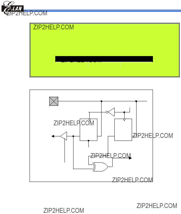
6.5.1.3Controller Reset Block Diagram
Fig.
(This specification is subject to change without further notice)
EM78P221/2N
6.5.2 The T and P Status under Status Register
A reset condition is initiated by one of the following events:
1.
2./RESET pin input "low"
3.WDT
The values of T and P as listed in the table below, are used to check how the processor wakes up.
* P: Previous status before reset
The following shows the events that may affect the status of T and P.
* P: Previous value before reset
(This specification is subject to change without further notice)

EM78P221/2N
6.6 Interrupt
The EM78P221/2N has four interrupts as listed below:
1.TCC overflow interrupt
2.Port 6 Input Status Change Interrupt
3.External interrupt INT0, INT1
4.When the Comparator 1 output status changes
Before the Port 6 Input Status Change Interrupt is enabled, reading Port 6 (e.g., "MOV R6, R6") is necessary. Each Port 6 pin will have this feature if its status changes. Port 6 Input Status Change Interrupt will wake up the EM78P221/2N from sleep mode if it is enabled prior to going into sleep mode by executing SLEP. When
The external interrupt has a
During a power source unstable situation, like during external power noise interference or EMS test condition, it will cause the power to vibrate fiercely. While Vdd is still unsettled, the supply voltage may be below working voltage. When the system supply voltage Vdd is below the working voltage, the IC kernel must automatically keep all register status.
Bank
When interrupt mask bits is ???Enable???, the flag in the Interrupt Status Register (RF) is set regardless of the ENI execution. Note that the result of Bank
When any interrupt occurs, the contents of ACC, R1 (Bits 5, 4, 1, 0), R3 (Bits 2 ~0), R4 registers are pushed to the corresponding stack (Fig
(This specification is subject to change without further notice)

EM78P221/2N
Fig.
Fig.
(This specification is subject to change without further notice)

EM78P221/2N
6.7 Comparator
The EM78P221/2N has one comparator comprising of two analog inputs and one output. The comparator can be utilized to wake up the EM78P221/2N from sleep mode. The comparator circuit diagram is depicted in the figure below.
Fig.
6.7.1External Reference Signal
The analog signal presented at Cin??? compares to the signal at Cin+, and the digital output (CO) of the comparator is adjusted accordingly by taking the following notes into considerations:
NOTE
???The reference signal must be between Vss and Vdd.
???The reference voltage can be applied to either pin of the comparator.
???Threshold detector applications may be of the same reference.
???The comparator can operate from the same or different reference sources.
6.7.2Comparator Outputs
??The compared result is stored in the CMPOUT of Bank
??Bits 3 ~ 4 <CMPCOS1, CMPCOS0> of the Bank
Bank
(This specification is subject to change without further notice)
EM78P221/2N
NOTE
???The highest priority of P71/INT1/CO is INT1. When EIS1=0, the working type of P71/INT1/CO is determined by CMPCOS1 and CMPCOS2.
???The CO and P71of the P71/CO pins cannot be used at the same time.
???The P71/CO pin priority is as follows:
P71/INT1/CO Pin Priority
The following figure shows the Comparator Output block diagram.
Fig.
6.7.3Using a Comparator as an Operation Amplifier
6.7.3.1Bank
Bit 2 (CMPWE): Comparator
0= Disable Comparator
1= Enable Comparator
When the Comparator output status change is used to enter an interrupt vector or to
Bit 0 (CMPIF): Comparator interrupt flag. Set when a change occurs in the Comparator output. Reset by software
(This specification is subject to change without further notice)

EM78P221/2N
6.7.3.2Bank
6.7.3.3Bank
Bit 0 (CMPIE): CMPIF interrupt enable bit 0 = Disable CMPIF interrupt 1 = Enable CMPIF interrupt
When the Comparator output status change is used to enter an interrupt vector or to enter the next instruction, the CMPIE bit must be set to ???Enable???. But actually the comparator output must be read to latch the status at first. Then the comparator output is compared to this latch to produce the information of output status change.
6.7.4 Comparator Interrupt
?? CMPIE must be enabled for the ???ENI??? instruction to take effect
?? Interrupt is triggered whenever a change occurs on the comparator output pin ?? The actual change on the pin can be determined by reading the Bit CMPOUT ?? CMPIF the comparator interrupt flag, can only be cleared by software
6.7.5
??If enabled, the comparator remains active and the interrupt remains functional, even in Sleep mode.
??If a mismatch occurs, the interrupt will wake up the device from Sleep mode.
??The power consumption should be taken into consideration for the benefit of energy conservation.
??If the function is unemployed during Sleep mode, turn off the comparator before entering sleep mode.
(This specification is subject to change without further notice)

EM78P221/2N
6.8 Oscillator
6.8.1 Oscillator Modes
The EM78P221/2N can be operated in six different oscillator modes, such as High Crystal oscillator mode (HXT 1, 2), Low Crystal oscillator mode (LXT 1, 2), External RC oscillator mode (ERC), and RC oscillator mode with Internal RC oscillator (IRC). Select one of such modes by programming the OSC2, OCS1, and OSC0 in the Code Option register.
The Oscillator modes defined by OSC2, OCS1, and OSC0 are described below.
1In ERC mode, OSCI is used as oscillator pin. OSCO/P52 is defined by code option Word 0 Bit 6 ~ Bit 4.
2In IRC mode, P53 is normal I/O pin. OSCO/P52 is defined by code option Word 0 Bit 6 ~ Bit 4.
3In LXT1, LXT2, HXT1 and HXT2 modes; OSCI and OSCO are used as oscillator pins. These pins cannot and should not be defined as normal I/O pins.
The maximum operating frequency limit of the crystal/resonator at different VDDs, are as follows:
6.8.2 Crystal Oscillator/Ceramic Resonators (Crystal)
The EM78P221/2N can be driven by an external clock signal through the OSCO pin as illustrated below.
OSCI
Ext.
Clock in
OSCO  Clock out
Fig.
(This specification is subject to change without further notice)

EM78P221/2N
In most applications, Pin OSCI and Pin OSCO can be connected with a crystal or ceramic resonator to generate oscillation. Fig.
Fig.
The following table provides the recommended values for C1 and C2. Since each resonator has its own attribute, user should refer to the resonator specifications for appropriate values of C1 and C2. RS, a serial resistor, may be required for AT strip cut crystal or low frequency mode. Fig
Capacitor selection guide for crystal oscillator or ceramic resonators:
(This specification is subject to change without further notice)

EM78P221/2N
Fig.
(This specification is subject to change without further notice)

EM78P221/2N
6.8.3External RC Oscillator Mode
For some applications that do not require precise timing calculation, the RC oscillator (Fig.
Vcc
Rext
OSCI
Cext
Fig.
In order to maintain a stable system frequency, the values of the Cext should not be less than 20pF, and the value of Rext should not be greater than 1M??. If the frequency cannot be kept within this range, the frequency can be easily affected by noise, humidity, and leakage.
The smaller the Rext in the RC oscillator, the faster its frequency will be. On the contrary, for very low Rext values, for instance, 1 K??, the oscillator will become unstable because the NMOS cannot discharge the capacitance current correctly.
Based on the above reasons, it must be kept in mind that all the supply voltage, the operation temperature, the components of the RC oscillator, the package types, and the PCB is layout, have certain effect on the system frequency.
The RC Oscillator frequencies:
(This specification is subject to change without further notice)
EM78P221/2N
6.8.4Internal RC Oscillator Mode
The EM78P221/2N offers a versatile internal RC mode with default frequency value of 4MHz. Internal RC oscillator mode has other frequencies (1MHz, 16MHz, and 455kHz) that can be set by Code Option (Word 1), RCM1, and RCM0. The Table below describes the EM78P221/2N internal RC drift with the variations on voltage, temperature, and process.
Internal RC Drift Rate (Ta=25??C, VDD=5.0V ?? 5%, VSS=0V)
Theoretical values are for reference only. Actual values may vary depending on actual process.
6.9
Any microcontroller is not warranted to start operating properly before the power supply stabilizes to a steady state. EM78P221/2N has a
6.9.1External
supply has a slow power rise time. Since the current leakage from the /RESET pin is about ??5??A, it is recommended that R should not be greater than 40K. This way, the voltage at Pin /Reset is held below 0.2V. The diode (D) functions as a short circuit at
(This specification is subject to change without further notice)

EM78P221/2N
6.9.2Residual Voltage Protection
When the battery is replaced, device power Vdd is removed but residual voltage remains. The residual voltage may trip below Vdd minimum, but not to zero. This condition may cause a poor
VDD
VDD
33K
Q1 10K
10K
/RESET
Fig.
VDD
VDD
R1
Q1
/RESET
Fig.
6.10 Low Voltage Reset
Low voltage reset (LVR) is designed for unstable power situation, such as external power noise interference or in EMS test condition.
When LVR is enabled, the system supply voltage (Vdd) drops below Vdd reset level (VRESET) and remains at 10??s, system reset will occur and the system will remain at reset status. The system will remain at reset status until Vdd voltage rises above Vdd release level. Refer to Fig
(This specification is subject to change without further notice)
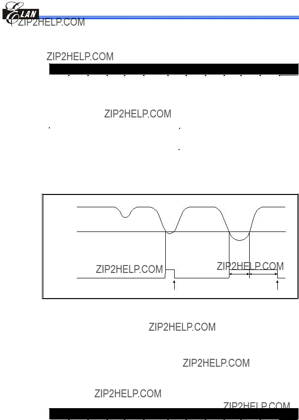
EM78P221/2N
LVR characteristics are set at Code Option Word 0, Bits 10 and 9. Detailed operation mode is as follows:
Word 0
Bits 10~9 (LVR1 ~ LVR0): Low Voltage Reset enable bits. If Vdd has crossover at Vdd reset level as Vdd changes, the system will reset.
Fig.
6.11 Code Option
EM78P221/2N has two Code Option Words and one Customer ID word that are not a part of the normal program memory.
6.11.1 Code Option Register (Word 0)
Word 0
(This specification is subject to change without further notice)

EM78P221/2N
Bits 12 ~ 11 (Type 1, Type 0): Type selection for EM78P221N or EM78P222N
Note: LVR1 and LVR0 are at Bank
Bits 10 ~ 9 (LVR1 ~ LVR0): Low Voltage Reset control bits
Bit 8 (CLKS): Instruction time period option bit 0 = two oscillator time periods
1 = four oscillator time periods (Default) Refer to Section 6.12 for Instruction Set
Bit 7 (ENWDTB): Watchdog timer enable bit 0 = Enable
1 = Disable (default)
Bits 6, 5 & 4 (OSC2, OSC1 & OSC0): Oscillator Mode Selection bits
1In ERC mode, OSCI is used as oscillator pin. OSCO/P52 is defined by code option Word 0 Bit 6 ~ Bit 4.
2In IRC mode, P53 is normal I/O pin. OSCO/P52 is defined by code option Word 0 Bit 6 ~ Bit 4.
3In LXT1, LXT2, HXT1 and HXT2 modes; OSCI and OSCO are used as oscillator pins. These pins cannot and should not be defined as normal I/O pins.
Bit 3: Not used (Reserved). This bit is set to 0 all the time
Bits 2 ~ 0 (PR2 ~ PR0): Protect Bits
PR2 ~ PR0 are protect bits. Each protect status is as follows:
(This specification is subject to change without further notice)

EM78P221/2N
6.11.2 Code Option Register (Word 1)
Word 1
Bit 12: Not used (reserved), fixed to ???1??? all the time.
Bit 11: Not used (reserved), fixed to ???0??? all the time.
Bit 10 (RESETENB): P81/RESET pin select bit 0 = P81 set as /RESET pin
1 = P81 is general purpose input pin or open drain for output port
(Default)
Bit 9 (RCOUT): System clock output enable bit in IRC or ERC mode 0 = OSCO pin is open drain
1 = OSCO output instruction clock (Default)
Bit 8 (NRHL): Noise rejection high/low pulse define bit. INT pin has a falling edge trigger.
0 = Pulses equal to 8/fc are regarded as signal
1 = Pulses equal to 32/fc are regarded as signal (Default)
NOTE
NRHL and NRE are at Bank
Bit 7 (NRE): Noise rejection enable
0 = disable noise rejection
1 = enable noise rejection (default). However in Low Crystal oscillator (LXT2) mode, the noise rejection circuit is always disabled.
NOTE
The noise rejection function is turned off in LXT2 and sleep mode.
Bit 6: Not used (Reserved). This bit is set to ???1??? all the time.
NOTE
C3, C2, C1, C0, RCM1 and RCM0 are at Bank
Bits 5~2 (C3~C0): Internal RC mode Calibration bits. These bits must always be set to ???1??? only (auto calibration)
(This specification is subject to change without further notice)

EM78P221/2N
Bit 1 & Bit 0 (RCM1 & RCM0): RC mode selection bits
6.11.3 Customer ID Register (Word 2)
Bit 12: Not used (reserved), fixed to ???0??? all the time
Bit 11 (NRM):
0 = Noise reject Mode 2. For
1 = Noise reject Mode 1. For General input or output use. (Default) Bits 10~9: Not used (reserved), fixed to ???1??? all the time
Bits 8 ~ 0: Customer???s ID code
6.12 Instruction Set
Each instruction in the instruction set is a
In addition, the instruction set has the following features:
1.Every bit of any register can be set, cleared, or tested directly.
2.The I/O registers can be regarded as general registers. That is, the same instruction can operate on I/O registers.
Convention:
R = Register designator that specifies which one of the registers (including operation and general purpose registers) is to be utilized by the instruction.
b = Bit field designator that selects the value for the bit located in the register R and which affects the operation.
k = 8 or
(This specification is subject to change without further notice)

EM78P221/2N
(This specification is subject to change without further notice)

EM78P221/2N
Note: 1 This instruction is not recommended for RF operation
2 This instruction cannot operate under RF.
(This specification is subject to change without further notice)

EM78P221/2N
(This specification is subject to change without further notice)

EM78P221/2N
Internal RC Electrical Characteristics (Ta=25??C, VDD=5 V, VSS=0V)
Internal RC Electrical Characteristics
(This specification is subject to change without further notice)
EM78P221/2N
8.1 Comparator (OP) Characteristic
Vdd = 5.0V, Vss=0V, Ta=25??C
Note: 1. The output voltage is in the unit gain circuitry and over the full input
2. The input
3. The response time specified is a 100mV input step with 5mV overdrive.
9 AC Electrical Characteristic
Ta=25??C, VDD=5V??5%, VSS=0V
Note: *N = selected prescaler ratio
(This specification is subject to change without further notice)
EM78P221/2N
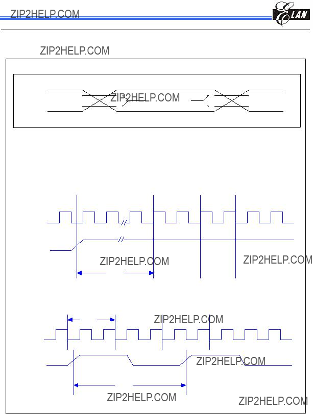
10 Timing Diagrams
AC Test Input/Output Waveform
AC Testing : Input is driven at
RESET Timing (CLK="0")
CLK
/RESET
Tdrh
TCC Input Timing (CLKS="0")
Tins
CLK
TCC
Ttcc
(This specification is subject to change without further notice)

EM78P221/2N
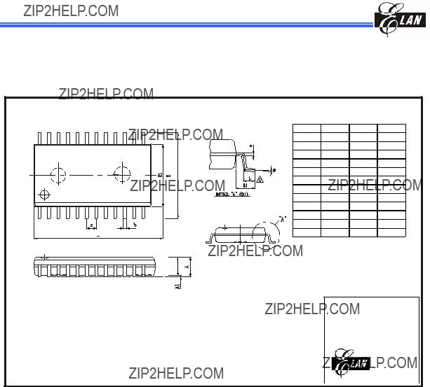
APPENDIX
A Package Type
Green products do not contain hazardous substances.
The third edition of Sony
Pb contents should be less than 100ppm
Pb contents comply with Sony specs.
(This specification is subject to change without further notice)

EM78P221/2N
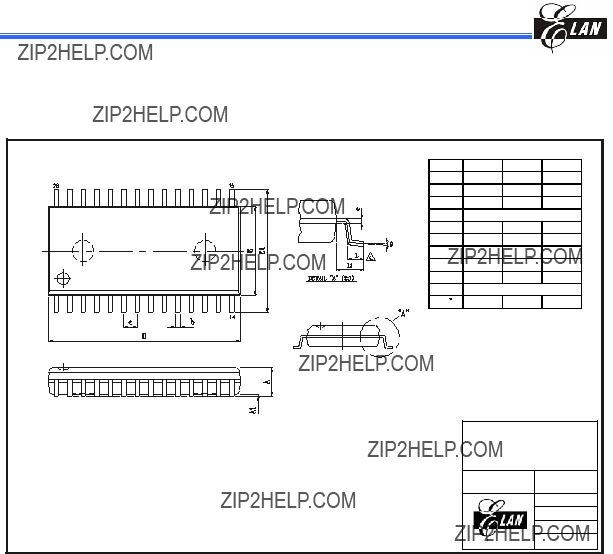
B Packaging Configuration
(This specification is subject to change without further notice)

EM78P221/2N
(This specification is subject to change without further notice)
EM78P221/2N
B.3
TITLE:
OUTLINE DIMENSION
(This specification is subject to change without further notice)

EM78P221/2N
B.4 28- Lead Plastic Skinny Dual in line (SDIP) ??? 300 mil
A
TITLE:
PACKAGE OUTLINE
DIMENSION
(This specification is subject to change without further notice)
EM78P221/2N
(This specification is subject to change without further notice)

EM78P221/2N
(This specification is subject to change without further notice)

EM78P221/2N
C Quality Assurance and Reliability
C.1 Address Trap Detect
An address trap detect is one of the MCU embedded
(This specification is subject to change without further notice)
