EM78M611E
???????????????????????????????????????????????????????????????
???????????????????????? ?????????????????????????????????????????????
Product
Specification
DOC. VERSION 1.1
ELAN MICROELECTRONICS CORP.
November 2006
EM78M611E
???????????????????????????????????????????????????????????????
???????????????????????? ?????????????????????????????????????????????
Product
Specification
DOC. VERSION 1.1
ELAN MICROELECTRONICS CORP.
November 2006
Trademark Acknowledgments:
IBM is a registered trademark and PS/2 is a trademark of IBM. Windows is a trademark of Microsoft Corporation.
ELAN and ELAN logo  are trademarks of ELAN Microelectronics Corporation.
Copyright ?? 2006 by ELAN Microelectronics Corporation
All Rights Reserved
Printed in Taiwan
The contents of this specification are subject to change without further notice. ELAN Microelectronics assumes no responsibility concerning the accuracy, adequacy, or completeness of this specification. ELAN Microelectronics makes no commitment to update, or to keep current the information and material contained in this specification. Such information and material may change to conform to each confirmed order.
In no event shall ELAN Microelectronics be made responsible for any claims attributed to errors, omissions, or other inaccuracies in the information or material contained in this specification. ELAN Microelectronics shall not be liable for direct, indirect, special incidental, or consequential damages arising from the use of such information or material.
The software (if any) described in this specification is furnished under a license or nondisclosure agreement, and may be used or copied only in accordance with the terms of such agreement.
ELAN Microelectronics products are not intended for use in life support appliances, devices, or systems. Use of ELAN Microelectronics product in such applications is not supported and is prohibited.
NO PART OF THIS SPECIFICATION MAY BE REPRODUCED OR TRANSMITTED IN ANY FORM OR BY
ANY MEANS WITHOUT THE EXPRESSED WRITTEN PERMISSION OF ELAN MICROELECTRONICS.
??? ?????? ??? ????????? ?????? ??? ??? ??? ?????? ??? ??? ??? ??? ??? ?????? ???????????? ??? ??? ??? ??? ??? ??? ??? ?????? ??? ???

Contents
???????????????????????????

Contents
APPENDIX
Specification Revision History

EM78M611E
Universal Serial Bus Series Microcontroller
1 General Description
The EM78611E is a series of
The EM78611E has
These series of ICs have many powerful features, including:
???Dual clock mode which allows the device to run on low power saving frequency.
???Pattern Detect Application function which is used in a serial transmission to count waveform width.
???Pause Width Modulation that can generate a
???
2Features
???Operating voltage: 4.4V ~ 5.5V
???
???USB Specification Compliance
???Universal Serial Bus Specification Version 1.1
???USB Device Class Definition for Human Interface Device (HID), Firmware Specification Version 1.1
???Supports one device address and three endpoints
???USB Application
???P75
???USB protocol handling
???USB device state handling
???Identifying and decoding of Standard USB commands to EndPoint Zero
???PS/2 Application Support
???
(This specification is subject to change without further notice)

EM78M611E
Universal Serial Bus Series Microcontroller
???
???
???
???Six available interrupts
???
???Two independent programmable prescalers for WDT and TCC
???Two power saving methods:
1.
2.Dual clock mode
???Two clocks per instruction cycle
???
???I/O Ports
???Up to 11 LED sink pins
???Each GPIO pin of Ports 5, 6, 8, P90~P93, P95 and P96; has an internal programmable
???Each GPIO pin of Port 6, P74 ~ P77 and Port 9 can wake up the MCU from sleep mode by input state change
???Internal Memory
???
???
???
???
???Operation Frequency
???Normal Mode: MCU runs with an external oscillator frequency of 6 MHz or 12 MHz
???Dual Clock Mode: MCU runs at a frequency of 256kHz (or 32 kHz, 4kHz, 500Hz), emitted by the internal oscillator with the external ceramic resonator turned off to save power.
???
???
???Up to 2 channels PWM function on P92 (PWM1) and P93 (PWM2)
???Up to
???Up to 8 selections of duty cycles
(This specification is subject to change without further notice)

EM78M611E
Universal Serial Bus Series Microcontroller
???
???Up to 24 channels
???Up to 10 bits resolution
???4 ADC conversion rates: 256K/128K/64K/32K
???
???For MCU power supply
???
???Package Type:
???
???
???
???
???
???
3 Type Definition
The EM78M611E series has six types of packaging. Each type is divided into two modules, namely; original, and with both E2PROM and A/D Converter. Hence, packaging configuration for each series is defined. Table 3.1 below summarizes which series of the EM78M611E belong to which module.
Table
4Application
???USB Keyboard only
???USB and PS/2 both compatible with Keyboard
???USB Keyboard with USB Mouse
???USB Joystick
(This specification is subject to change without further notice)

EM78M611E
Universal Serial Bus Series Microcontroller
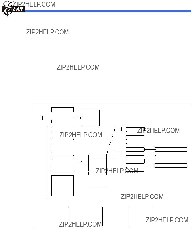
5 Pin Assignment
(This specification is subject to change without further notice)

EM78M611E
Universal Serial Bus Series Microcontroller
Fig.
Fig.
(This specification is subject to change without further notice)

EM78M611E
Universal Serial Bus Series Microcontroller
(This specification is subject to change without further notice)
EM78M611E
Universal Serial Bus Series Microcontroller
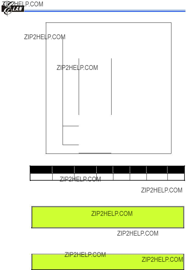
7 Block Diagram
DATA & CONTROL BUS
(This specification is subject to change without further notice)

EM78M611E
Universal Serial Bus Series Microcontroller
8 Function Description
The EM78M611E memory is organized into three spaces, namely; User Program memory in 6K??13 bits ROM space, Data Memory in 144 bytes SRAM space, EEPROM space and USB Application FIFOs for EndPoint0, EndPoint1, and EndPoint2. Furthermore, several registers are used for special purposes.
8.1 Program Memory
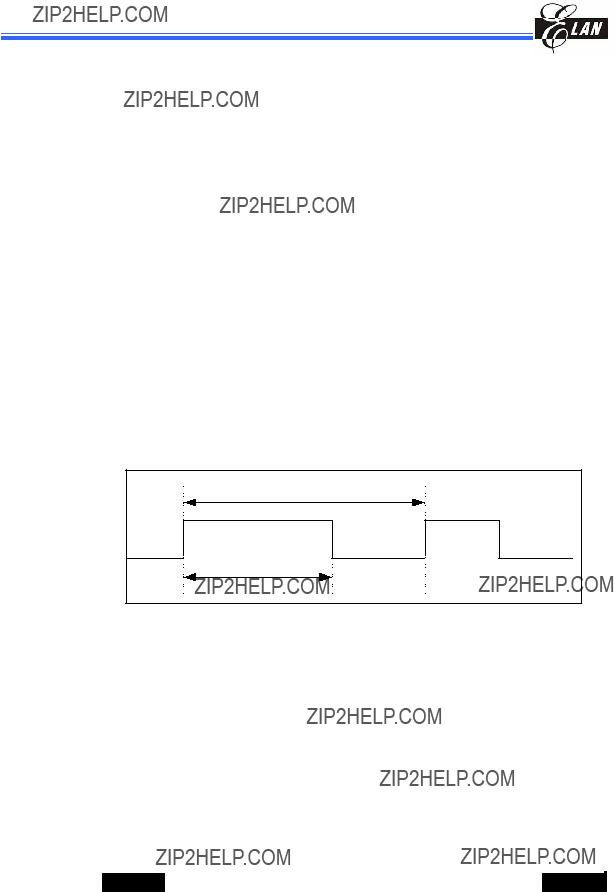
The program space of the EM78M611E is 6K words, and is divided into six pages. Each page is 1K words long. After a reset, the
The Interrupt Vector is at 0x0001 and accommodates TCC interrupt, RF1 (SE1) timing counter interrupt, RF2 (SE2) timing counter interrupt, P74~P77 State Changed interrupt, EndPoint0 interrupt, USB Suspend interrupt, USB Reset interrupt, and USB Host Resume interrupt.
After an interrupt, the MCU will fetch the next instruction from the corresponding address as illustrated in the following diagram.
(This specification is subject to change without further notice)
EM78M611E
Universal Serial Bus Series Microcontroller
8.2 Data Memory
The Data Memory has 144 bytes SRAM space. It has also an
8.2.1 Special Purpose Register
When the microcontroller executes instructions, specific registers are implemented to ensure proper operation of essential functions such as Status Register which records the calculation status, Port I/O Control Registers which control the I/O pins??? direction, etc. Lots of other special purpose registers are provided for various functions.
Note that Special Control Registers can only be read or written to by two instructions: IOR and IOW.
(This specification is subject to change without further notice)

EM78M611E
Universal Serial Bus Series Microcontroller
8.2.2 Operation Registers
The following subsections describe each of the Operation Registers of the Special Purpose Registers. The Operation Registers are arranged according to the order of the registers??? address. Note that some registers are read only, while others are both readable and writable.
8.2.2.1R0 (Indirect Addressing Register) Default Value: (0B_0000_0000)
R0 is not a physically implemented register. Its major function is as an indirect addressing pointer. Any instruction using R0 as a pointer actually accesses data pointed by the RAM Select Register (R4).
8.2.2.2R1 (Timer / Clock Counter) Default Value: (0B_0000_0000)
The TCC register is an
8.2.2.3R2 (Program Counter & Stack) Default Value: (0B_0000_0000)
The EM78M611E Program Counter is a
(This specification is subject to change without further notice)
EM78M611E
Universal Serial Bus Series Microcontroller
13FF
1400
Page 0
17FF
8.2.2.4R3 (Status Register) Default Value:(0B_0001_1XXX)
R3 [0] Carry/Borrow Flag
0 = No
1 = A
NOTE
For Borrow, the polarity is reversed. For rotate (RRC, RLC) instructions, this bit is loaded with either high or
R3 [1] Auxiliary Carry/Borrow Flag. For ADD, SUB Instructions
0 = No
1 = A
NOTE
For Borrow, the polarity is reversed.
(This specification is subject to change without further notice)

EM78M611E
Universal Serial Bus Series Microcontroller
R3 [2] Zero flag. It will be set to 1 when the result of an arithmetic or logic operation is zero.
R3 [3] Power down flag. It will be set to 1 during
0: Power down
1:
R3 [4]
0: Watchdog timer overflow occurs
1: No Watchdog timer overflow
The various states of Power down flag and
0*P WDT
10 Power down mode
*P: Previous status before WDT reset
R3
(This specification is subject to change without further notice)
EM78M611E
Universal Serial Bus Series Microcontroller
8.2.2.5R4 (RAM Select Register) Default Value: (0B_00XX_XXXX)
R4 (RAM select register) contains the address of the registers.
R4 [0~5] used to select registers in 0x00h~0x3Fh. The address 0x00~0x1F is common space. After 0x1Fh, SRAM is divided into four banks, using Bank Select Register.
R4 [6, 7] used to select the registers bank (refer to the table below). The following are two examples:
(1)R4=00001100 and R4=10001100 point to the same register 0x0Ch. Since 0x0Ch is in the common space, Bit 6 and Bit 7 are meaningless.
(2)R4=10111100 points to the register 0x3C in Bank 2.
(This specification is subject to change without further notice)

EM78M611E
Universal Serial Bus Series Microcontroller
8.2.2.11 RA (EEPROM Control Register) Default Value: (0B_1111_1111)
RA is a command register for EEPROM control. For detailed usage of this register, refer to Section 8.2.3 which describes the EEPROM embedded in the EM78M611E.
8.2.2.12RB (Pattern Detect Application Control Register)
Default Value: (0B_0000_0000)
RB is a control register for controlling the Pattern Detect Application function. For detailed description of this register, refer to Section 8.7.2 which describes the PDA function.
RC [0] Stall flag. While the MCU receives an unsupported command or invalid parameters from host, this bit will be set to 1 by the firmware to notify the UDC to return a STALL handshake. When a successful Setup transaction is received, this bit is cleared automatically. T his bit is readable and writable.
RC [1] EP0_Busy flag. When this bit is equal to ???1,??? it indicates that the UDC is writing data into the EP0???FIFO or reading data from it. During this time, the firmware will avoid accessing the FIFO until UDC finishes writing or reading. This bit is only readable.
RC [2] Host Suspend flag. If this bit is equal to 1, it indicates that USB bus has no traffic for a specified period of 3.0 ms. This bit will also be cleared automatically when there is bus activity. This bit is only readable.
RC [3] EP2_W flag. This bit is set when the UDC receives a successful data from USB Host to EP2. Upon detecting that this bit is equal to one, the firmware will execute a read sequence to the EP2???s FIFO, after which this bit is cleared. Otherwise, the subsequent data from USB Host won???t be accepted by the UDC.
RC [4, 5, 6] EP0_R / EP1_R / EP2_R flag. These three bits inform the UDC to read the data from the FIFO. Then the UDC will send the data to the Host automatically. After UDC finishes reading the data from the FIFO, this bit will be cleared automatically.
Therefore, before writing data into FIFO???s, the firmware will first check this bit to avoid overwriting the data. These three bits can only be set by firmware and cleared by hardware.
RC [7] EP0_W flag. After the UDC completes writing data to the FIFO, this bit will be set automatically. The firmware will clear it as soon as it gets the data from EP0???s FIFO. Only when this bit is cleared that the UDC will be able to write a new data into the FIFO.
Therefore, before the firmware can write data into the FIFO, this bit must first be set by the firmware to prevent the UDC from writing data at the same time. This bit is both readable and writable.
(This specification is subject to change without further notice)
EM78M611E
Universal Serial Bus Series Microcontroller
8.2.2.12RD (USB Application FIFO Address Register)
Default Value: (0B_0000_0000)
RD [0~4] USB Application FIFO address registers. These five bits are the address pointers of USB Application FIFO.
RD [5~7] Undefined registers. The default value is zero.
8.2.2.13RE (USB Application FIFO Data Register)
Default Value: (0B_0000_0000)
RE (USB Application FIFO data register) contains the data in the register of which address is pointed by RD.
NOTE
For example, if user wants to read the fourth byte of EndPoint Zero, user has to use the address of EP0 (0x00) and Data Byte Pointer of EP0 (0x10) to access it.
//Read the 4th byte of the EP0 FIFO
//First, assign the data byte pointer of EP0 register (0X10) with 0X03. MOVA, @0X10
MOVRD, a // Move data in A to RD register MOVA, @0X03
MOVRE , A // Move data in A to RE register
//Then read the content from EP0 FIFO (0x00) 4th byte
MOVA, @0X00
MOVRD, A // Assign address point to EP0 FIFO
MOVA, RE // Read the fourth byte data (Byte 3) of the EP0 FIFO
MOV A, 0X0E// Read the fifth byte data (Byte 4) of the EP0 FIFO
RF [0] TCC Overflow interrupt flag. It will be set while TCC overflows, and is cleared by firmware.
RF [1] EndPoint Zero interrupt flag. It will be set when the EM78M611E receives Vendor/Customer Command to EndPoint Zero. This bit is cleared by firmware.
(This specification is subject to change without further notice)
EM78M611E
Universal Serial Bus Series Microcontroller
RF [2] USB Suspend interrupt flag. It will be set when the EM78M611E finds the USB Suspend Signal on USB bus. This bit is cleared by the firmware.
RF [3] USB Reset interrupt flag. It will be set when the host issues the USB Reset signal.
RF [4] P74/P75/P76/P77 Port state change interrupt flag.
In PS2 Mode, only pins configured as inputs can cause this interrupt to occur. These pins (P74, P75, P76 and P77) are compared with the value latched on the last read of Port 7.
In USB Mode, P76 and P77 have this function.
NOTE
R F[4]: Port State Change Interrupt Flag,
EM78M611
USB Mode
PS2 Mode ??? P74/P75/P76/P77 have interrupt function.
EM78M611E
P74/P75/P76/P77 all have interrupt function (in USB & PS2 mode)
RF [5, 6] SE1 / SE2 Pattern Detect Interrupt flag. These two flags are used for Pattern detect application.
RF [7] USB Host Resume interrupt flag. It will be set only in Dual clock mode when the USB suspend signal becomes low.
NOTE
RF [7]: USB Host Resume_IF
In EM78M611, this bit is always ???1???. It is not for use.
In EM78M611E, this bit is O.K. for use.
8.2.3 Control Registers
Some special purpose registers are available for special control purposes. Except for the Accumulator (ACC), these registers must be read and written with special instructions. One of these registers, CONT, can only be read by the instruction "CONTR" and written by "CONTW" instruction. The other special control registers can be read by the instruction "IOR" and written by the instruction "IOW".
The following paragraphs describe only the general functions of the control registers.
8.2.3.1A (Accumulator)
The accumulator is an
(This specification is subject to change without further notice)
EM78M611E
Universal Serial Bus Series Microcontroller
8.2.3.2CONT (Control Register) Default Value: (0B_0011_1111)
Except for Bit 6 (Interrupt enable control bit), the CONT register can be read by the instruction "CONTR" and written by the instruction ???CONTW".
CONT [0~2] Watchdog Timer prescaler bits. These three bits are used as the Watchdog Timer prescaler.
CONT [3~5] TCC Timer prescaler bits.
The relationship between the prescaler value and these bits are shown below:
NOTE
WDT Timing base is
Ex. Code option [2 ,1] = 01 (2ms), and Prescaler = 1:128.
WDT overflow time is: 2mS * 2^7 = 256 mS
CONT [6] Interrupt enable control bit. This bit toggles Interrupt function between enable and disable. It is set to 1 by the interrupt disable instruction "DISI" and reset by the interrupt enable instructions "ENI" or "RETI."
0 : Disable the Interrupt function
1 : Enable the Interrupt function
CONT [7] LED bit. This bit is used to enable the LED sink capacity of P76 and P77.
0 : Disable the LED sink capacity of P76, P77
1 : Enable the LED sink capacity of P76, P77
(This specification is subject to change without further notice)

EM78M611E
Universal Serial Bus Series Microcontroller
8.2.3.3IOC5 ~IOC9 I/O (Port Direction Control Registers)
Default Value: (0B_1111_1111)
These are I/O port (Port 5 ~ Port 7) direction control registers. Each bit controls the I/O direction of three I/O ports respectively. When these bits are set to 1, the relative I/O pins become input pins. Similarly, the I/O pins becomes outputs when the relative control bits are cleared.
0 : Output direction
1 : Input direction
8.2.3.4IOCA (Operation Mode Control Register) Default Value: (0B_1110_0000)
IOCA [0, 1] These two bits are used to select the operation mode.
0 : Do Not support remote wake up
1 : Supports remote wake up
NOTE
IOCA[4]: Remote_Wake up bit
EM78M611 do NOT support this function. Only EM78M611E does.
(This specification is subject to change without further notice)

EM78M611E
Universal Serial Bus Series Microcontroller
IOCA [6, 7] Select the operation frequency in Dual Clock Mode. Four frequencies are available and can be chosen as Dual Clock Mode in running the MCU program.
8.2.3.5IOCB (Port 9
Default Value: (0B_X111_1111)
IOCB [0~6] These bits are used to select which of the Port 9 pins is to be assigned to wake up the MCU while in Power down mode.
0 : Enable the function
1 : Disable the function
8.2.3.6IOCC (Port 9 LED Sink Capacity Control Register)
Default Value: (0B_X00X_0000)
IOCC [0~3, 5, 6] LED sink control bit. These bits are used to enable the LED sink capacity of P90 ~ P97
0 : Disable the LED sink capacity of respective pin
1 : Enable the LED sink capacity of respective pin
IOCC [4, 7] Reserved bits
8.2.3.7IOCD (Port 9 Pull High Control Register) Default Value: (0B_X11X_1111)
IOCD [0~3, 5, 6] These bits control the 25K??
0 : Enable the
1 : Disable the
IOCD [4, 7] Reserved bits
(This specification is subject to change without further notice)
EM78M611E
Universal Serial Bus Series Microcontroller
8.2.3.8IOCE (Special Function Control Register) Default Value: (0B_1101_0111)
IOCE [0, 1, 2] Port 5, Port 6, and Port 8
1 : Disable
IOCE [3] Setting this bit will allow the UDC to execute resume signaling. This bit is set by firmware to generate a signal to
NOTE
IOCE[3]: Device_Resume bit
In EM78M611, this bit is always ???0???. It is not for use.
In EM78M611E, this bit is O.K. for use.
IOCE [4] Run bit. This bit can be cleared by firmware and set during
0 : Sleep mode. The EM78M611E is in power down mode.
1 : Run mode. The EM78M611E is working normally.
IOCE [5] Watchdog Timer enable bit. The bit disables/enables the Watchdog Timer.
0 : Disable WDT
1 : Enable WDT
IOCE [6] Enable the
0 : Enable the
1 : Disable the
IOCE [7] Dual clock Control bit. This bit is used to select the frequency of system clock. When this bit is cleared, the MCU will run on very low frequency for power saving and the UDC will stop working.
0 : Selects to run on slow frequency
1 : Selects EM78M611E to run on normal frequency
(This specification is subject to change without further notice)

EM78M611E
Universal Serial Bus Series Microcontroller
8.2.3.9IOCF (Interrupt Mask Register) Default Value J(0B_0000_0000)
IOCF [0~7] TCC / EP0 / USB Suspend / USB Reset / Port 7 State Change / SE1_IE / SE2_IE / USB Host Resume interrupt enable bits. These eight bits control the TCC interrupt function, EP0 interrupt, USB Suspend interrupt, USB Reset interrupt, Port 7 State Change interrupt and USB Host Resume interrupt respectively. Individual interrupt is enabled by setting its associated control bit in the IOCF to "1."
0 : Disable Interrupt
1 : Enable Interrupt
Only when the global interrupt is enabled by the ENI instruction will the individual interrupt work. After DISI instruction, any interrupt will not work even if the respective control bits of IOCF are set to 1.
The USB Host Resume Interrupt works only in Dual clock mode. This is because when the MCU is in sleep mode, it will be automatically woken up by the UDC Resume signal.
8.3 Extra Control Register
Five extra control registers are available to control some special functions. The five registers are ERA (AD Control register), ERB (AD_LSB), ERC (AD_MSB), ERD (AD_Rate), and ERE (PWM Control register)
Remember to set IOCA[3] before accessing these five registers. The operating method is the same as with other control registers.
8.4 USB Application FIFOs
For USB Application, EM78M611E provides an
(This specification is subject to change without further notice)

EM78M611E
Universal Serial Bus Series Microcontroller
8.5 USB Application
EM78M611E is designed specially for USB device application and has many powerful functions that support the firmware to free itself from complex situation in various aspects of USB application.
8.5.1 USB Device Controller
The EM78M611E
The UDC handles and decodes most Standard USB commands defined in the USB Specification Rev1.1. If the UDC receives an unsupported command, it will set a flag to notify the MCU of the receipt of such command. The Standard Commands that the EM78M611E supports includes; Clear Feature, Get Configuration, Get Interface,
Get Status, Set Address, Set Configuration, Set Feature, and Set Interface.
Each time the UDC receives a USB command, it writes the command into the EP0???s FIFO. Only when it receives unsupported command will the UDC notify the MCU through interrupt.
Hence, the EM78M611E is very flexible under USB application since the developer can freely choose the method of decoding the USB command as dictated by different situation.
(This specification is subject to change without further notice)

EM78M611E
Universal Serial Bus Series Microcontroller
8.5.2 Device Address and Endpoints
EM78M611E supports one device address and three endpoints, EP0 for control endpoint, EP1 and EP2 for interrupt endpoint. Sending data to USB host in EM78M611E is very easy. Just write data into EP???s FIFO, then set flag, and the UDC will handle the rest. It will then confirm that the USB host has received the correct data from EM78M611E.
8.6 Reset
The EM78M611E provides three types of reset: (1)
8.6.1
a.The program counter is cleared.
b.The TCC timer and Watchdog timer are cleared.
c.Special registers and Special Control registers are all set to their initial values.
8.6.2 Watchdog Reset
When the Watchdog timer overflows, it causes the Watchdog to reset. After it resets, the program is executed from the beginning and some registers will be reset. The UDC however, remains unaffected.
8.6.3 USB Reset
When the UDC detects a USB Reset signal on the USB Bus, an MCU interrupt occurs, after which it proceeds to perform the specified process that follows. After a USB device is attached to the USB port, it cannot respond to any bus transactions until it receives a USB Reset signal from the bus.
8.7 Saving Power Mode
The EM78M611E provides two options of
8.7.1 Power Down Mode
The EM78M611E enters into Power Down mode by clearing the RUN register (IOCE[4]). During this mode, the oscillator is turned off and the MCU goes to sleep. It will wake up when signal from USB host is resumed, or when a Watchdog reset occurs or when an input port state changes.
If the MCU wakes up when I/O port status changes, the direction of the I/O port should be set at input direction, and then read the state of port. For example:
(This specification is subject to change without further notice)

EM78M611E
Universal Serial Bus Series Microcontroller
:
// Set the Port 6 to input port
IOW PORT6
// Read the state of Port 6
The EM78M611E has one internal oscillator for power saving application. Clearing the Bit IOCE [7] will enable the low frequency oscillator. At the same time, the external oscillator will be turned off. Then the MCU will run under very low frequency to conserve power. Four types of frequency are available for selection in setting bits IOCA [6, 7].
The USB Host Resume Interrupt can only be used in this mode. If this interrupt is enabled, the MCU will be interrupted when the USB Host Resume signal is detected on USB Bus.
8.8 Interrupt
The EM78M611E has one interrupt vector in 0x0001. When an interrupt occurs during an MCU program run, it will jump to the interrupt vector (0x0001) and execute the instructions sequentially from the interrupt vector. RF is the interrupt status register, which records the interrupt status in the relative flags/bits.
The interrupt condition could be one of the following:
TCC Overflow: When the Timer Clock / Counter Register (R1) overflows, the status flag RF[0] will be set to 1. Its interrupt vector is 0X0001.
Port 7 State Change: When the input signals in Port 7 changes, the status flag RF[4] will be set to 1. Its interrupt vector is 0X0001.
SE1 Pattern Detection Interrupt Conditions: If the Pattern Detection Application function is enabled, there will be four conditions with which interrupt is generated, and the status flag RF[5] is set to 1 (interrupt vector is 0X0001).
a)Signal from P.92 changes to low and the Pattern Counter value is bigger than R11 register value.
(This specification is subject to change without further notice)

EM78M611E
Universal Serial Bus Series Microcontroller
b)Signal from P.92 changes to high, and Pattern Counter value bigger than R10 register value.
c)P.92 remains high, and the Pattern Counter value is equal to 0XFF.
d)P.92 remains low, and the Pattern Counter value is equal to 0XFF.
SE2 Pattern Counter Interrupt Conditions: If the Pattern Detection Application function is enabled, there will be three conditions with which interrupt is generated and the status flag RF[6] is set to 1(interrupt vector is 0X0001).
a)Signal from P.93 changes to low and the Pattern Counter value is bigger than R13 register value.
b)Signal from P.93 changes to high and the Pattern Counter value is bigger than R12 register value.
c)P.93 remains high, and the Pattern Counter value is equal to 0XFF.
d)P.93 remains low, and the Pattern Counter value is equal to 0XFF.
EP0 interrupt: When the UDC successfully accepts a setup transaction from host to EndPoint0, the status flag RF[1] is set to 1. Its interrupt vector is 0X0001.
USB suspend: When UDC detects a USB Suspend signal on the USB bus, the status flag RF[2] is set to 1. Its interrupt vector is 0X0001.
USB Reset: When the UDC detects a USB Reset signal on the USB bus, the status flag R[3] is set to 1. Its interrupt vector is 0X0001.
USB Host Resume: When the UDC detects that the USB bus is no longer in Suspend condition and without Device Resume signal, the status flag R[7] is set to 1. Its interrupt vector is 0X0001.
IOCF is an interrupt mask register which can be set bit by bit. While their respective bit is written to 0, the hardware interrupt will inhibit, that is, the EM78M611E will not jump to the interrupt vector to execute instructions. But the interrupt status flags still records the conditions no matter whether the interrupt is masked or not. The interrupt status flags must be cleared by firmware before leaving the interrupt service routine and enabling other interrupt.
The global interrupt is enabled by the ENI (RETI) instruction and is disabled by the DISI instruction.
8.9 Pattern Detect Application (PDA)
8.9.1 Function Description
This function is designed for the serial signal transmission, e.g., the transmission between a wireless device and its receiver box. The EM78M611 has two sets of
(This specification is subject to change without further notice)

EM78M611E
Universal Serial Bus Series Microcontroller
Pattern Detect Application (PDA) can calculate the length of one pattern and interrupt the MCU while the serial signal is transiting from high to low (or
8.9.2 Control Register
The PDA includes an enable control bit, one control register and
IOCA [2] PDA Enable Control Bit
When this bit is set, the PDA function starts and the P92 and P93 become input pin automatically to sample the serial signal.
0 : disable PDA function
1 : enable PDA function
RB (PDA Control Register) Default Value: (0B_0000_0000)
This register is used to define two parameters of PDA function; signal sampling rate and debounce length. When a pattern ends, the value in the counter is loaded into its respective register and the RB[6] or RB[7] is set to indicate which type of pattern (high or low) is at its end or which type of pattern counter is on overflow.
0: low pattern
1: high pattern
R10 (P.92 Low Pattern Counter)
This register records the length of P.92 in low status.
R11 (P.92 High Pattern Counter)
This register records the length of P.92 in high status.
R12 (P.93 Low Pattern Counter)
This register record the length of P.93 in low status.
R13 (P.93 High Pattern Counter)
This register records the length of P.93 in high status.
R10~R13 function as general registers if this function is not enabled. Once the enabled bit is set, these four registers will be loaded with the value of the pattern counter.
8.9.3 Sampling Rate and Debounce Length
Although the
The PDA samples the serial signal every fixed interval. The pattern counter will be incremented by one at sampling time if the signal remains unchanged. If the signal is at
(This specification is subject to change without further notice)
EM78M611E
Universal Serial Bus Series Microcontroller
high state, then the ???high pattern counter??? will increase; otherwise the ???low pattern counter??? increases. As long as the signal state changes, the PDA will debounce signal and load the value of pattern counter into the respectively register for the firmware to read. For example, if the signal in P.92 is in ???low??? state, the low counter of P.92 will count continuously until the state of the input signal in P.92 changes. When a state change occurs (in this case, the signal changes from ???low??? to ???high??? state), the PDA will take a time break (which is equal to the result of sampling interval multiplied by the debounce length), to avoid possible noise. After the debounce length time, if the signal remains in high state, the high pattern counter will start to count and load the low pattern counter???s value into R10. At the same time, RB[6] is cleared to indicate that low pattern is over.
The correlation between the control register value and debounce time are as follows:
On the other hand, when the signal of P92 always remains ???low???, the low pattern counter of P92 will eventually overflow. Once the counter overflows, the content of the counter will also be loaded into R10, that is, the register is written to 0xFF, and the counter is reset to count from zero again.
If the hardware interrupt of PDA function is enabled, (IOCF[5] is equal to ???1???), then the program will go to 0x0001 to execute interrupt routine while the content of a pattern counter is loaded into the register.
The correlation between the value of control register and actual sampling rate are as shown below:
(This specification is subject to change without further notice)
EM78M611E
Universal Serial Bus Series Microcontroller
After the PDA function is enabled (by setting IOCA[2] to 1), user can write a default value to the High Pattern counter register and Low Pattern counter register. Then set the corresponding interrupt enable bit (IOCF[5]). When the counting value of one ???H??? pattern is bigger than the default value of R11, the Pattern Detecting interrupt will be generated. Similarly, if the counting value of one ???L??? pattern is bigger than the default value of R10, Low Pattern Detecting interrupt will occur. Thus, the EM78M611 is notified and aware that one effective pattern is received from P.92.
If user does not need these two interrupts, they can be masked. The new value of counting a pattern will still be loaded to the R10 and R11. The firmware must poll and determine whether the value of these two registers has changed or not.
8.10 Pulse Width Modulation (PWM)
8.10.1 Function Description
In PWM mode, both PWM1 (P.92) and PWM2 (P.93) produce plus programmable signal of up to 8 bits resolution.
The PWM Period is defined as 0xFF ?? Timer Counter Clock. The Timer Counter clock source is controlled by an extra control register, ERE. For example; if the Clock source is 1MHz, then the Period will be 255 ??seconds.
Fig.
8.10.2 Duty Cycle
The PWM duty cycle is defined by writing to the R10/R11 Register for PWM1/PWM2.
Duty Cycle = ( R10 / 255 ) ?? 100% for PWM1 ( R11 / 255 ) ?? 100% for PWM2
8.10.3 Control Register
R10 (PWM1 Duty Cycle Register)
A specified value keeps the output of PWM1 to remain at high for a Period.
R11 (PWM2 Duty Cycle Register)
A specified value keeps the output of PWM2 to remain at high for a Period.
ERE(PWM Control Register) Default Value: (0B_0000_0001)
(This specification is subject to change without further notice)

EM78M611E
Universal Serial Bus Series Microcontroller
ERE [0~2] PWM Clock Prescaler
ERE [6, 7] PWM1/PWM2 Enable Bit
0 : Disable
1 : Enable
8.11
8.11.1 Function Description
The Analog to Digital converter consists of a
The ADC module utilizes successive approximation to convert the unknown analog signal to a digital value. The result is fed to the ADDATA. Input channels are selected by the analog input multiplexer via the ADCS/RAS bits AD0~AD4.
Start
Full
Conversion Time: 12 clock time of internal clock source
8.11.2 Control Register
ERA (AD Channel Select Register) Default Value: (0B_0001_1111)
(This specification is subject to change without further notice)

EM78M611E
Universal Serial Bus Series Microcontroller
ERA [0~4]: AD Channel Selector
ERA [7] AD Converter ready flag
0 ??? 1: Start AD Conversion (set by firmware).
1 ??? 0: When AD conversion is finished and has moved digital data into the AD Data Register, this bit will be set by hardware.
NOTE
Hardware can enable this function only at AD Channel Select of the functional I/O port. After a
ERB (AD LSB Data Register) Default Value: (0B_0000_0000)
(This specification is subject to change without further notice)

EM78M611E
Universal Serial Bus Series Microcontroller
ERC (AD MSB Data Register) Default Value: (0B_0000_0000)
2 bits AD MSB Digital Data.
ERD (AD Control Register) Default Value: (0B_0000_0000)
ERD [0 1]: The clock source of AD converting time.
00: 256kHz
01: 128kHz
10:64kHz
11:32kHz
8.12EEPROM
Four bytes of EEPROM are located in the R2C~R2F of Bank 3. The stored data of EEPROM are not erased when the power is off and can be read and
A control register, ERA controls the EEPROM, that is, to read, write, or to erase the data from EEPROM. Writing a command into this register will execute an action to the EEPROM. The command value is defined in the following tale. Note that there is an execution time laps for each command. Before writing the next command into the control register, allow enough time for the EEPROM to finish the previous command.
(This specification is subject to change without further notice)

EM78M611E
Universal Serial Bus Series Microcontroller
9 Absolute Maximum Ratings
10 DC Electrical Characteristic
T = 25??C, VDD=5V, VSS=0V
(This specification is subject to change without further notice)

EM78M611E
Universal Serial Bus Series Microcontroller
(This specification is subject to change without further notice)
EM78M611E
Universal Serial Bus Series Microcontroller
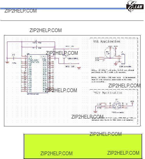
11 Application Circuit
NOTE
A.BC1 , BC2 : load Capacitor
B.C1 (bypass capacitor) : that placed adjacent to VDD pin , to minimize noise.
C.C2 , C3 (power capacitor) : that placed adjacent to the Power source , will improve transient response and ripple rejection.
(This specification is subject to change without further notice)

EM78M611E
Universal Serial Bus Series Microcontroller
APPENDIX
A Special Register Map
Operation Registers
(This specification is subject to change without further notice)

EM78M611E
Universal Serial Bus Series Microcontroller
Control Registers
Extra Register (IOCA[3] = 1)
(This specification is subject to change without further notice)
EM78M611E
Universal Serial Bus Series Microcontroller
B Instruction Set
Each instruction in the instruction set is a
(a)Executing the instruction "MOV R2, A", "ADD R2,A", "TBL", or any other instructions that write to R2 (e.g. "SUB R2,A", "BS R2,6", "CLR R2", ????????????).
(b)Execute CALL, RET, RETI, RETL, JMP, Conditional skip (JBS, JBC, JZ, JZA, DJZ, DJZA) which were tested to be true.
Under these cases, the execution takes two instruction cycles. In addition, the instruction set has the following features:
(1). Every bit of any register can be set, cleared, or tested directly.
(2). The I/O register can be regarded as general register. That is, the same instruction can operate on I/O register.
Legend:
R = Register designator that specifies which one of the 64 registers (including operation and general purpose registers) is to be utilized by the instruction.
Bits 6 and 7 in R4 determine the selected register bank.
b = Bit field designator that selects the value for the bit located in the register R and which affects the operation.
k = 8 or
(This specification is subject to change without further notice)

EM78M611E
Universal Serial Bus Series Microcontroller
Note: 1 This instruction is applicable to IOCx only.
2 This instruction is not recommended for RE, RF operation.
(This specification is subject to change without further notice)

EM78M611E
Universal Serial Bus Series Microcontroller
C Code Option Register
EM78M611E has two Code option registers, which are not part of the normal program memory. The option bits cannot be accessed during normal program execution.
Address 000:
Address 001:
Address 000:
Bit 1 (Frequency) : Frequency Selection
0 : MCU run on 12 MHz
1 : MCU run on 6 MHz
Bits 3~2 (OST_1 ~ OST_0) : Oscillator
00 : 500??s
01 : 2ms
10 : 8ms
11 : 16ms
Bits 4~12 : User ID
Address 001:
Bits 1~0 (Package_1 ~ Package_0) : Package type selection
00 : Not defined
01 : 40 pins
10 : Not defined
11 : 44 pins
Bits 3~2 : Reserved bits
(This specification is subject to change without further notice)

EM78M611E
Universal Serial Bus Series Microcontroller
Bit 4 (/R.S.) : D-
0 : Connect Resistor Switch
1 : Disconnect Resistor Switch
Bit 5 (/AD_Hold) : Halts the MCU during AD conversion
0 : Halts the MCU during AD conversion
1 : MCU keeps running during AD conversion
Bit 6 (EP2_Enable) : Endpoint 2 Enable
0 : Disable
1 : Enable
Bit 7 (EP2_Dir) : Endpoint 2 Direction
0 : OUT
1 : IN
Bits 10~8 (EP2_Maxsize_2~0) : Endpoint 2 maximum size
000 : 1 Byte
001 : 2 Bytes
010 : 3 Bytes
011 : 4 Bytes
100 : 5 Byte
101 : 6 Bytes
110 : 7 Bytes
111 : 8 Bytes
Bits 12~11: Values are fixed
(This specification is subject to change without further notice)